Continue to Site

Welcome to EDAboard.com

Welcome to our site! EDAboard.com is an international Electronics Discussion Forum focused on EDA software, circuits, schematics, books, theory, papers, asic, pld, 8051, DSP, Network, RF, Analog Design, PCB, Service Manuals... and a whole lot more! To participate you need to register. Registration is free. Click here to register now.

How to use Synthesizer PLL ICs with Integrated VCO to make harmonic VCO (x2 x4 x8..)?

Status
Not open for further replies.

Terminator3

Advanced Member level 3
Joined
Feb 25, 2012
Messages
802
Helped
71
Reputation
142
Reaction score
63
Trophy points
1,308
Activity points
9,027
How to use Synthesizer PLL ICs with Integrated VCO to make harmonic VCO(6GHz->24Ghz)?

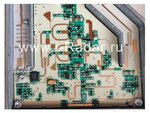
Hello all! I have recently seen some blurry photo of K-band VCO.
Most importantly, instead of traditional DRO/microstrip resonator or some kind of Hititte VCO chip, or some multi-stage multiplier there was something different:
vco-design.png
i think it is some pretty damn simple yet cost effective 6GHz to 24GHz multiplier!

There is a pretty huge chip, i suspect something like LTC6946, LTC6948 (VCO+PLL). Also there is smaller chip, i think it is ATMEL or something to configure VCO+PLL chip.
1) VCO+PLL single chip (something around ~6GHz)
2) Some transition part to optimize x4 harmonics
3) Clearly it is 24GHz band-pass filter,
4,5) Two-stage amplifier to amplify 24GHz
6) Receiving antenna single-stage amplifier
7) Rat-race balanced mixer (schottky diodes)

I am pretty sure, that (1) chip is not 24GHz, and not even 12GHz. Although it may be 12GHz, but i still feel that it is something cheaper.

As you can see, two-stage amplifier (4,5) have no any filtering, so it is not multi-stage multiplier. The only band-pass filter is (3), and it is clearly final frequency here, just very weak before amplified.

Here is transition between some low-frequency chip (green part) and K-band part (white part):
pll-vco-multiplier.png
It is most important thing i want to understand in this design. There is two black chips, looks like diodes or transistors. It is unknown. PLL+VCO chips usually have balanced output, so I suspect here signal is summed up somehow, so balanced output x4 harmonic is in-phase.

Also it can be push-push VCO with PLL chip, but i still hope it is something more interesting

If you have any thoughts about this design, please comment! Thanks!
 
Last edited:
Looks like a 12 GHz push-push VCO, having the 2nd harmonic (24 GHz) going to the Divider/PLL.
 
By 12GHz push-push VCO do you mean two 6GHz oscillators in push-push configuration, resulting in 12GHz frequency and 24GHz harmonic amplified by two FETs? Also 6GHz goes to PLL chip.

Or two 12GHz oscillators in push-push configuration, with 24GHz harmonic? 12GHz goes to divider/PLL...

I mean what is the lowest frequency used here? I think that PLL is 6GHz. Because if two black things "2" is push-push oscillator, then i do not see any resonating network for 12GHz. But at 6GHz i believe it can be lumped.

- - - Updated - - -

I checked that image again.
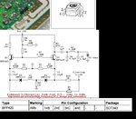
bfp420.jpg
it looks like push-push oscillator using BFP420 and some lumbed components.
BFP420 pin 3 used (collector) for output.
 

UPDATE: configuration of push-push oscillator seems similar to https://www.eevblog.com/forum/repair/radar-detector-teardown-and-look-inside/
I looked through photos on eevblog, and can't understand where is 180deg phase shift or common oscillator is.
Here is some images of push-push oscillators used in radar detectors:
push-push-oscillators.jpg
Third and fourth maybe have some lumped common resonator. But first and second oscillators does not seem to have common resonator. How it works here? I read many papers about push-push oscillators, and all of them (2-push at least) provide 180 deg phase shift through resonator (common resonator).
 
Last edited:

The push-push oscillator (nr 2 in your picture) https://i.imgur.com/jPy52wZ.jpg use two SiGe transistors BFP405 (ALs) and the printed resonator is the big circle between them.
The main characteristic of the push-push oscillators is that they can cancel the fundamental fo getting at the output only the 2nd harmonic 2fo. The resonator actually resonate on fo.
So using components working fine at fo you get a signal at 2fo, method which is very helpful in microwaves. Is even cheaper than using a frequency doubler.
 
Thank for your reply! I marked base, emitter and collector here:
push-push2.jpg
Also some related patents:
http://www.freepatentsonline.com/5402087.html
http://www.freepatentsonline.com/7388537.html (this is US7388537, linked to US5402087)
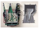
UPDATE: image of radar detector PCB with two push-push oscillators (exact US7388537):
1380136689_1-zolotye-dorozhki-v-rupore.jpg1380136754_10-plata-rupor-v-razbore.jpg

I read that circle line is common resonator (lambda/2 or 180deg at F0), and 2*F0 signal is taken from center, where signals F0 are out of phase, and 2*F0 harmonic is in-phase. There are some details in patents. But nothing about reflection coefficient design.

How to design one arm of such oscillator? Can i design one arm of such oscillator as series feedback, by deleting second transistor part? This design reminds me N-push oscillator with ring resonator. There was interesting papers on 4-push, 8-push oscillators with ring in center, all series feedback.

Also: http://www.taconic-add.com/en/pdf/technicalarticles--antiphase_design_for_balanced-oscillators.pdf
balanced oscillator design, something very similar.
 
Last edited:

If you remove one transistor, the circuit is not push-push anymore. Only using two active components you can get this approach.
Most of the push-push oscillator types are not feedback oscillators, and they are negative resistance oscillators.
 
If course i understand that. My idea is to design simple 6GHz series feedback oscillator first (knowing that it will be used in push-push later). Then use this 6GHz oscillator as building block of push-push oscillator with 12GHz output. It is pretty easy with coupled resonator, but here "circle" resonator is directly attached to BJT's emitters. I am unsure how it should be treated, probably not open-circuit.

- - - Updated - - -

This paper gives some insight: https://amsacta.unibo.it/1341/1/GA052158.PDF
push-push.png
For the analysis of a push-push oscillator we cut the
circuit at its symmetry line and investigate the odd mode
and the even mode operation individually. In the odd
mode equivalent circuit the suboscillator is terminated
by a virtual ground.

So for 12 GHz push-push we can design 6GHz negative resistance oscillator with quarterwave drain stub, which terminated with virtual ground (so it becomes half-wave open-stub).

but i can't understand why:
n the even mode equivalent circuit the suboscillator is
terminated by twice the load impedance 2 · ZL.
Why it be terminated with twice of the load impedance (2 x ZL)? Why not just ZL?
Maybe because they made 2 x ZL lines before power combining it to ZL final load line?
 

Please comment on my idea:
For example, we need very cheap VCO to make linear sweeps (high linearity) to measure distance. As sweep time is relatively small, can we use this approach:
1. make microstrip oscillator with fixed frequency OSCfixed=4.5 GHz (of course it will float over time, but during short period of time, say few milliseconds, it can be assumed constant)
2. make microstrip VCO with altering frequency OSCvco=5.0GHZ ... 5.1GHz

3. put diode mixer between OSCfixed and OSCvco to obtain frequency difference, that will be always greater than 1.5GHz and less than 1.6GHz.

4. put mixer output to some cheap PLL chip (with freq <2.4GHz), use PLL chip output to control OSCvco.

Disadvantages? feasibility?
 

Your approach mixing two LOs should work fine.
Or you can use a PLL on 2.5 GHz, and use a frequency doubler, because this would eliminate the mixer and a second LO.
 
vfone, thank for your reply!
adf4158, it is very good IC, comes with software. I am learning it now.

Can we use Integer-N PLL (ADF4106) to implement 50MHz linear frequency sweep at 5GHz frequency? Whould it be linear while switching channels, and what would be sweep time? As i understand, channel spacing must be very small, and we must constantly send control registers to switch between channels.

In case of Integer-N PLL should i
1) Choose R counter such that Fr equals to channel step (channel step is such that we can sweep 50MHz in required time, it depends on how fast i can send registers to ADF4106 and how fast it react)
2) Send registers to get N=B*P+A and control VCO to get on Fvco=N*Fr frequency

or

1) Change reference frequency with required saw-tooth waveform
2) One time send registers for fixed frequency. As reference frequency changes, VCO frequency will be changed according to reference frequency
 
Last edited:

I don't know if you can use ADF4106 to implement a sweeper for FMCW radar.
From what I know in FMCW you need milliseconds for a full frequency sweep.
Have to ask ADI which is the best option for you, and meantime you can play with their PLL software ADIsimPLL to check for the frequency sweep options:
https://form.analog.com/Form_Pages/RFComms/ADISimPll.aspx
 
Thank you, i downloaded this software already, and the other specifically designed for adf4158.
ADF4158 is ideal solution. ADF4106 is cheap, more convenient for radios. For linear chirp main difficulty is transition between channel switching and data port speed. I learned recently, that if i feed reference with DDS, there are phase noise problems. With ADF4158 we do not need DDS.
 

If you manage to design the FMCW radar using ADF4158 on 5GHz (with 100MHz BW), please post here a message that everything works fine.
 

Status
Not open for further replies.

Part and Inventory Search

Welcome to EDABoard.com

Sponsor

Back
Top