wfg42438
Member level 3
- Joined
- Jun 29, 2015
- Messages
- 54
- Helped
- 0
- Reputation
- 0
- Reaction score
- 0
- Trophy points
- 6
- Location
- California
- Activity points
- 620
Hello ,
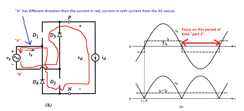
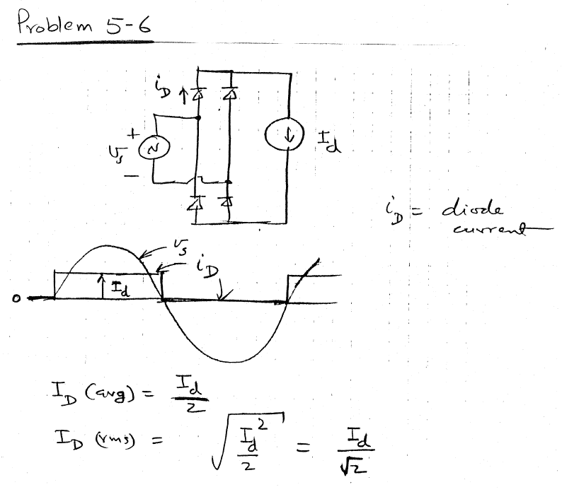
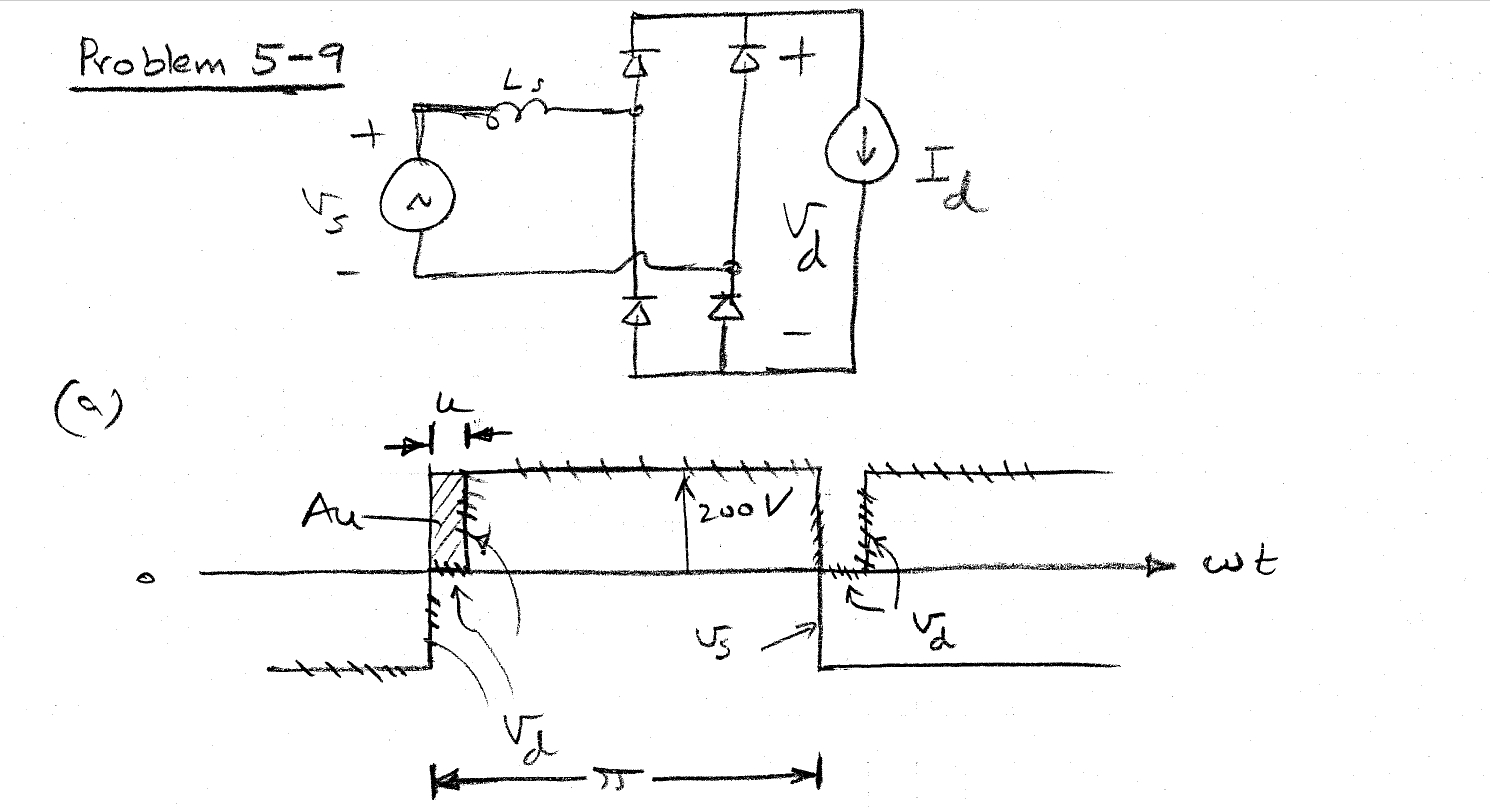
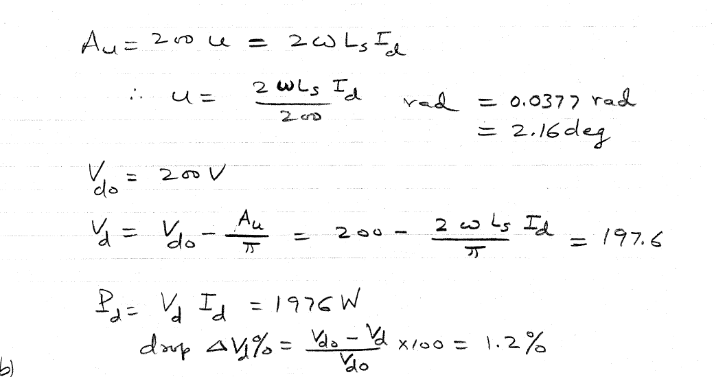
Can someone please explain why the current at the output is considered to a pulse??
I don't understand how this the case if out input voltage is sinusoidal, or is the pulse obtained not necessarily the output?
Please refer to the document and the schematic attached
https://user.unob.cz/leuchter/Mohan_usmernovace.pdf