Electro nS
Full Member level 6
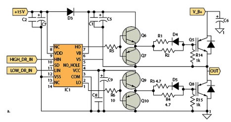
I am using the IR21844 in half bridge configuration , now i have to modify the circuit for a larger mosfet (2500nC gate charge total) , i would like to boost the output current into 4-5A ( from the original 1.4A) and keeping the same Driver since i donot want to change the logic side of the circuit.
IR mensions this in one of its appnote :
I would like to know if this circuit ( the 2 cascade totem poles ?) can be simplified more or replaced by IC that boosts the current.
IR mensions this in one of its appnote :
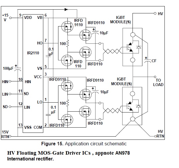
I would like to know if this circuit ( the 2 cascade totem poles ?) can be simplified more or replaced by IC that boosts the current.