Continue to Site

Welcome to EDAboard.com

Welcome to our site! EDAboard.com is an international Electronics Discussion Forum focused on EDA software, circuits, schematics, books, theory, papers, asic, pld, 8051, DSP, Network, RF, Analog Design, PCB, Service Manuals... and a whole lot more! To participate you need to register. Registration is free. Click here to register now.

Dc/dc buck converter variable output voltage

Status
Not open for further replies.

ginolas

Newbie level 4
Joined
Feb 11, 2016
Messages
7
Helped
0
Reputation
0
Reaction score
0
Trophy points
1
Activity points
55
Low current dc/dc converter for wireless transmitter/receiver

Hello,

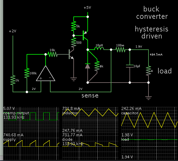
I have to conceive a dc/dc converter (buck), low power with a variable output voltage controled by analog signal in Bipolar or CMOS technology. Frequency: 1MHz, I: 500mA, the output varies between 1V to 3V.

Can someone help with an appropriate topology, some links or good advices please.

Kind regards,


Gino
 

Re: Low current dc/dc converter for wireless transmitter/receiver

Switched-coil converters are a popular topic at this forum. Try a search on 'buck converter'. You'll find many discussions, including schematics.
 
Hi,

I'd like to build a variable output DC/DC buck converter. the output varies in regard of a wave signal ( demodulated LTE signal). Does any body can help with the appropriate design and the list of equipment and tools needed to build it?

Kind regards,

Gino
 

Need for help dc/dc converter

CONVERTISSEUR_DC_DC.pngCONVERTISSEUR_DC_DC.png

Hello Everyone,

I just want to know how to make the output of this dc/dc buck converter variable. I want to have 1V-3V to the output as Vref is an analog signal. The output must be proportional to the analog signal.

image: https://obrazki.elektroda.pl/3721007200_1455816605.png

Thank you for your help,

Kind regards,

Gino
 

This simulation resembles your specs to some extent. I have tried a simpler version with real components. It works at low V and A. One op amp is all you need.


Adjust reference voltage (at left) to get your desired output V.

The 8k resistor is unnecessary. (It's there to make the simulation run smoothly.)

My design has an NPN driving a PNP, so that the output stage is referenced to 0V ground. If you wish, you can re-arrange it so the output is referenced to supply +. Then you only need one transistor.
 
Hi Brad,

Thank you for your help, i think I will use your schematic. Do you know circuit efficiency? Is it possible to rearrange the circuit to function with 3.5V batt instead of 5V batt? and if I put a variable signal at the reference, will the output follow?

Thanks again,

Gino
 

Hi Brad,

Your schematic is helpful. I want to know, if i want the circuit to work with a 3.5V instead of 5V how do I rearrange it? and if I put a sine at Vref, how do I guarantee a variable output between 1 to 3 V please.

Regards,
 

You may as well start experimenting on your own, either with a simulator or real components. Then you will find out whether you can get it to work at 3.5V, 500mA.

You can recognize the basic buck converter at the right half of my schematic. Everything else is the control circuit. The control circuit compares the output voltage to a reference voltage. When the output voltage drops too low, it switches on the PNP for a brief time, until the output voltage goes back up sufficiently.

The high gain of the control circuit is its chief utility. Also some hysteresis action. There is more than one component you can use for this. Obvious choices are an op amp or comparator. They are designed to perform such functions.

It may be possible to use a 555 timer IC, or logic gates, etc.
 
You want a converter that produces DC output...

This DC output will be proportional to some analog input...

Such a gadget is called an amplifier (input---> output; increased in current, voltage, power or admittance)

All amplifiers need power to amplify (sounds reasonable) but we do not describe it that way!

But what you are thinking is perhaps a class-D amplifier.

Am I missing something???
 

Hi c_mitra,

I just found out later that it is a dynamic power supply (DPS) for power amplifier for mobile phone. Output have to change according to the change of the envelope. I don't know if this help...

Best regards,

Gino
 

Your controller schematic isn't but a general template, you need to put in specific component combinations for Z1 and Z2 to make it an actual controller, e.g. a PI. You also need to correct the driver polarity to inverting for the present switcher topology.

There should be a specification of intended control behavior, particularly bandwidth of the setpoint signal and acceptable error band.

I just found out later that it is a dynamic power supply (DPS) for power amplifier for mobile phone. Output have to change according to the change of the envelope. I don't know if this help...
I presume it's a homework exercise, but it should contain a complete specification.
 
Hi Brad

Thank you for your advice. I downloaded a simulator to simulate the circuit...and I will try to improve it to get deisred result..

Best regards
 

I guess what you are designing is envelope tracking power amplifier (ETPA). There are many papers focusing on this topic.
 

Status
Not open for further replies.

Similar threads

Part and Inventory Search

Welcome to EDABoard.com

Sponsor

Back
Top