Continue to Site

Welcome to EDAboard.com

Welcome to our site! EDAboard.com is an international Electronics Discussion Forum focused on EDA software, circuits, schematics, books, theory, papers, asic, pld, 8051, DSP, Network, RF, Analog Design, PCB, Service Manuals... and a whole lot more! To participate you need to register. Registration is free. Click here to register now.

SIW Simulation using HFSS

Status
Not open for further replies.

arve9066

Member level 2
Joined
Jan 21, 2016
Messages
48
Helped
0
Reputation
0
Reaction score
0
Trophy points
6
Activity points
446
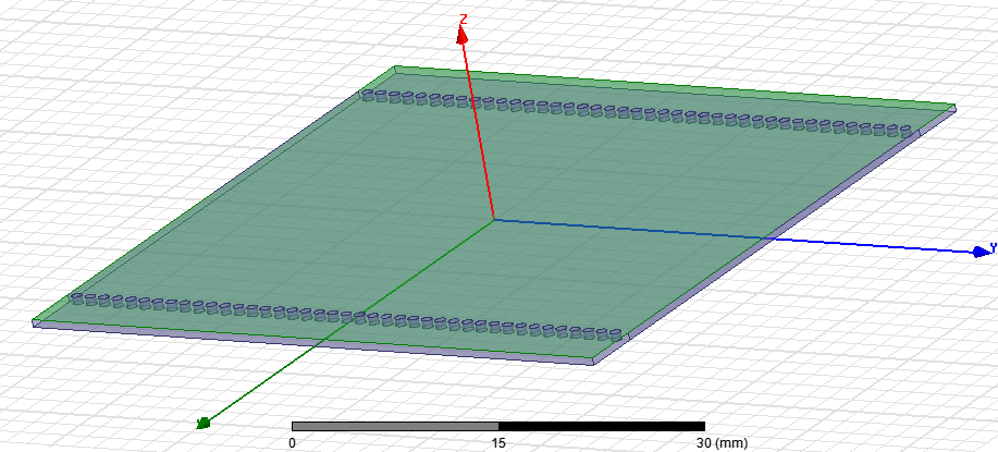
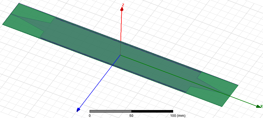
I am trying to simulate a Substrate Integrated Waveguide structure in HFSS at 2Ghz frequency. I need some help to set up the excitation and boundary conditions. I have a microstrip to SIW transition, SIW structure followed by a SIW to microstrip transition. Right now when I use a driven terminal approach with lumped ports I get the error that there is only one conductor in one of the ports which I kinda understand since the top and bottom planes are shorted through the via holes. So do I use only Driven modal with waveport excitation? Also do I need any air box or radiation boundary definitions when simulating this structure?
 

As long as you are using a waveport, be sure the excitation plane is on the edge of your simulation. A waveport is a port that simulates an infinitely long waveguide as the source. Could you include a picture of your simulation thus far? If you have vias or slits, then I would think you would want to include an airbox larger than your waveguide and assign there a radiation boundary.

As far as your error, I'm pretty sure you shouldn't get an error for the conductor being shorted elsewhere, that would prohibit simulating a lot of common structures. You probably will get an error without an integration line leading from one conductor to another on the plane of your excitation.
 

I removed the microstrip to SIW transition and was able to excite the SIW part alone using regular wave ports. That gives me the right results. So I guess the problem is with the microstrip to SIW transition. So I need to figure out a way to get that transition right. Find the images of both the setups I am using below


Also when I am simulating a guided structure like a waveguide what is the meaning of including a radiation boundary or an air box. Ideally the structure should not radiate right? The boundary conditions should take care of everything. I did not define it when simply simulating the SIW part alone which is just like a waveguide and it works just fine.
 

You won't have waveports on all sides of your simulation domain. What is above the above the upper surface?

While for a guided mode, the difference between a radiation boundary and a PEC can be small (perhaps negligibly so), generally one wants to avoid a situation where it may be a critical difference, and err on the side of caution.
 

The structure is a dielectric with two layers of copper on bottom and top faces. The bottom and top layers are shorted through the dielectric by array of metallic vias. I have defined waveports on the two faces (perpendicular to Y axis on the first pic) and defined modes. I did not define an airbox/radiation boundary, but the results were as expected. I had defined the via material as copper and the bottom and top layers are also copper. I selected all vias and set them as radiation boundary and that also as expected gave the same results.
 

Don't you have a MS to SIW transition? If you only actually have a completely covered dielectric, then yes, you don't need a radiation boundary at all, assuming the waveport covers the entire face on either end.

I selected all vias and set them as radiation boundary and that also as expected gave the same results.

I'm not sure what you mean "as expected". I wouldn't expect much from doing this... was there a particular reason?
 

Yeah.. I need to insert a MS to SIW transition. That's when its behaving weird.. So I do have to define a radiation boundary when I include the MS to SIW transition right?
 

Status
Not open for further replies.

Part and Inventory Search

Welcome to EDABoard.com

Sponsor

Back
Top