Continue to Site

Welcome to EDAboard.com

Welcome to our site! EDAboard.com is an international Electronics Discussion Forum focused on EDA software, circuits, schematics, books, theory, papers, asic, pld, 8051, DSP, Network, RF, Analog Design, PCB, Service Manuals... and a whole lot more! To participate you need to register. Registration is free. Click here to register now.

Reflection Oscillator Simulation

Status
Not open for further replies.

micro7311

Junior Member level 2
Joined
Jun 21, 2015
Messages
22
Helped
0
Reputation
0
Reaction score
0
Trophy points
1
Activity points
199
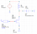
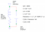
Hi, I am trying to simulate a reflection oscillator with a frequency of 4 GHz. Attached is my circuit and simulation plots. From what I understand from reflection oscillators, the resonator frequency is far below the oscillator output frequency. Here, my resonator frequency is ~3.268 GHz, which is not much below 4 GHz. Also, power output of the second harmonic is very close to the fundamental. The FET I am using is TOM1 model.

Could someone comment on this design and help optimize it? Thank you.
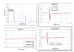
Plots.png**broken link removed**FET.pngResonator.png
 

You can add in series to the source a small inductor and a small capacitor in parallel. And pick the output signal from the source, where the signal is more sinusoidal (less harmonics) than from the drain.
The minimum level of harmonics you get if you pick the output signal directly from the resonator (using a coupler), but the level is lower, because the coupling cannot be tight.

https://people.engr.ncsu.edu/mbs/MicrowaveRFDesign/CS_Osc1/CS_Osc1_4up.pdf
 

Thank you I will try that. I am trying to understand the exact purpose for the need to tune the feedback TX line that is tied to the FET gate. Is it the parasitic capacitance and inductance of the transmission line that contributes to resonant frequency, which is why the oscillator output doesn't oscillate exactly at the resonator frequency?

Also, I noticed that there is only negative conductance locally around the center frequency when looking at the admittance chart. How much of the frequency spectrum should be negative conductance for an optimal design?

TL at the Gate supplies feedback to create a negative impedance for oscillations.The oscillator HB frequency is generally is found lower than Resonator theoritical resonance frequency due to some parasitic capacitive effects around the circuit.But your case seems a bit different because I think there are 2 resonance point in the circuit and HB catches the upper one.
 

Status
Not open for further replies.

Part and Inventory Search

Welcome to EDABoard.com

Sponsor

Back
Top