Shady Ahmed
Member level 5
Hi all,
I am designing a low drop out regulator, with the specifications of power supply rejection of -30 dB up to 10 MHz, with load current 2mA.
Using 0.13um technology and 1.8v Supply.
With 1V reference voltage generated from a NON IDEAL band gap circuit & using a NON IDEAL op amp. And the regulated voltage = 1.5v
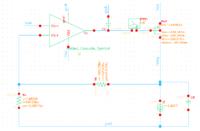
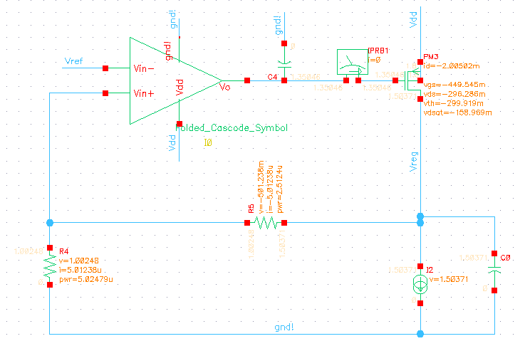
Here is my schematic:
My problem is that I don't understand the factors affecting the power supply rejection.
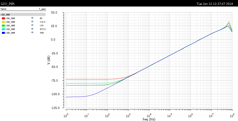
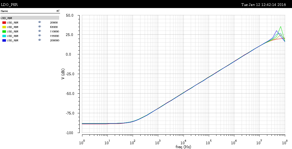
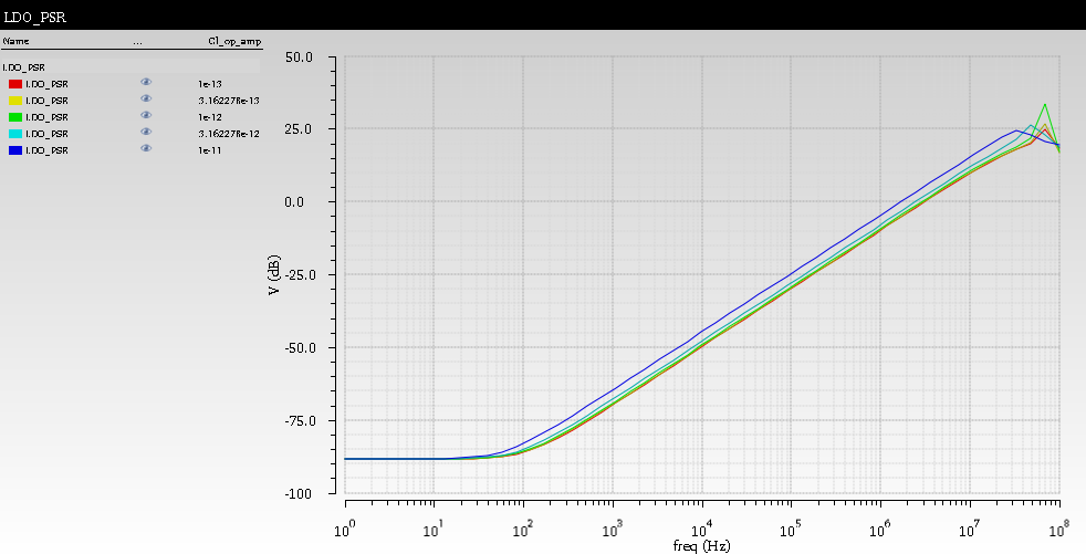
It starts at -60dB at DC, However it keeps increasing and exceeds 0 dB at the KHz range!!
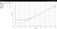
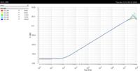
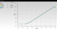
Here are 3 different graphs showing the PSR plots against 3 factors showing that it almost doesn't depend on any of them!
1- PSR against width of the pass transistor
2- PSR against the resistors value
3- PSR against the op amp load capacitance
Thanks for you time, and ur input is much appreciated.
I am designing a low drop out regulator, with the specifications of power supply rejection of -30 dB up to 10 MHz, with load current 2mA.
Using 0.13um technology and 1.8v Supply.
With 1V reference voltage generated from a NON IDEAL band gap circuit & using a NON IDEAL op amp. And the regulated voltage = 1.5v
Here is my schematic:
My problem is that I don't understand the factors affecting the power supply rejection.
It starts at -60dB at DC, However it keeps increasing and exceeds 0 dB at the KHz range!!
Here are 3 different graphs showing the PSR plots against 3 factors showing that it almost doesn't depend on any of them!
1- PSR against width of the pass transistor
2- PSR against the resistors value
3- PSR against the op amp load capacitance
Thanks for you time, and ur input is much appreciated.