Continue to Site

Welcome to EDAboard.com

Welcome to our site! EDAboard.com is an international Electronics Discussion Forum focused on EDA software, circuits, schematics, books, theory, papers, asic, pld, 8051, DSP, Network, RF, Analog Design, PCB, Service Manuals... and a whole lot more! To participate you need to register. Registration is free. Click here to register now.

Tuned amplifier: some conflicts

Status
Not open for further replies.

anhnha

Full Member level 6
Joined
Mar 8, 2012
Messages
322
Helped
4
Reputation
8
Reaction score
4
Trophy points
1,298
Activity points
3,684
This is a tuned amplifier. I have two problems hope anyone here could make them clear.


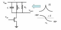
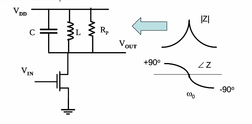
1. As we know the output voltage swings above VDD. I can explain it from summing of DC and small signals.
However, is there a physics explanation for that? I mean using characteristic of R, L, C components.

2. For DC analysis, assuming that Vin and VDD are fixed and Vin is chosen so that the transistor is always in saturation.
(Vth < Vin < VDD + Vth)

Now from square law equation, the current Id from D to S should be constant and independent with shape ration W/L.
Is that right?
 
Last edited by a moderator:

1) Output voltage can go up to 2VDD when output and supply are isolated using an inductive load. It's a simple fact that when you already have established VDD as quiescent point in the output, any signal with certain frequency will lead output to go above VDD.

2) Actually Id is a strong fucntion of W/L. Id=0.5*un*cox*(W/L)*OD*OD
OD is the overdrive voltage
 
  • Like
Reactions: anhnha

    anhnha

    Points: 2
    Helpful Answer Positive Rating
Thanks. For question no.2 I made a mistake in omitting W/L in formula.
However, with question no 1, I think you misunderstood my question. I can see why Vo can go up to 2VDD from DC and small signal as you said above. But I would like to know an physics explanation for that.
 

... I would like to know an physics explanation for that.
Current through an inductance cannot suddenly stop when the transistor goes off (closed). So an additional force (voltage) is necessarily be created to keep the current flowing until this voltage will be taken over by the capacitance and disintegrated by the resistance respectively.

Think of a super wave - a tsunami climbing up steep rocks. The height (≙ voltage) can reach a multiple of its original wave height.
 
  • Like
Reactions: anhnha

    anhnha

    Points: 2
    Helpful Answer Positive Rating
Hi,
In this case, the transistor never goes off. So how does that happen?
BTW, I simulated that in Cadence and get impedance phase start from -90 degree and and at -270 degree not +90 and -90 as in the picture.
Is there something wrong with that?
 

In this case, the transistor never goes off. So how does that happen?

Perhaps it doesn't fully get off, but may be it keeps a forced oscillation, concerning both voltage and current (with their phase shift). The drain side will see an oscillation voltage swinging between (nearly) GND and (nearly) the double VDD voltage at one maximum of the oscillation. The reason for this is the same as described above: When the transistor is (nearly) off, its drain voltage is (nearly) VDD, but the inductance will continue to "drive" its current so that the drain voltage will continue to rise up to (nearly) double the VDD value.

... I simulated that in Cadence and get impedance phase start from -90 degree and and at -270 degree not +90 and -90 as in the picture. Is there something wrong with that?
No, this doesn't matter, it's just a question of the chosen boundary condition (start condition).
 
  • Like
Reactions: anhnha

    anhnha

    Points: 2
    Helpful Answer Positive Rating
Thanks. I've got it now.

No, this doesn't matter, it's just a question of the chosen boundary condition (start condition).
Relating to this problem, I still not sure how can I choose the boundary condition here. I simulated it in Cadence not choose it myself.

- - - Updated - - -

And I have another question, hope you could make it clear.
I ran transient analysis with input vsin for frequencies like 1G, 2G,.. and the output is always at resonant frequency. Is there something wrong here?
I thought that output should have the same frequency as input.
 

... how can I choose the boundary condition here. I simulated it in Cadence not choose it myself.
It depends on the start phase of your stimulation source - if you use such. If not, the start phase (of a self-starting circuit) can be random.

I ran transient analysis with input vsin for frequencies like 1G, 2G,.. and the output is always at resonant frequency. Is there something wrong here? I thought that output should have the same frequency as input.
Depends on your circuit. Probably the resonant circuit forces the fundamental component of oscillation.
 

Status
Not open for further replies.

Part and Inventory Search

Welcome to EDABoard.com

Sponsor

Back
Top