mtwieg
Advanced Member level 6
I've been playing with the UMC 65nm PDK for designing low noise OTAs for operation from 100kHz-10MHz, and have found that the noise simulation results change in strange ways depending on what device models I choose. In particular I'm comparing twp low threshold 1.2V pmos types, one regular and one RF version. And the RF version has an optional thermal noise enhancement flag, which changes the results as well, so that means there are three variations in total.
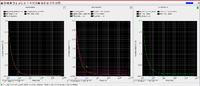
So I compare all three variations with identical drain bias current and voltage (strong inversion, saturated), and same W and L. The DC operating points, including Vgs and gm, are very similar, but the noise results are not. Below (left to right) shows plots of drain current spot noise from the normal pmos, the RF pmos with thermal enhancement, and the RF pmos without thermal enhancement.
So at 1MHz, the normal pmos has the highest noise, while RF pmos is lower, especially without the noise enhancement (which is even less than theory would predict). At 100kHz, the difference between normal and RF PMOS is even greater.
From what I understand, the normal and RF varieties aren't really different devices (same doping, same oxide, etc), but using the RF device models in my schematic means that when moving to layout I will automatically get cells optimized for noise, which is nice. But when I simulate based on RF models at low-ish frequencies, can my results be trusted?
To further compound the issue, I will actually be biasing the transistors very close to subthreshold, but the model documents say that the RF thermal noise enhancements are not valid for Vgs<0.45V. I have seen that under these conditions, the RF models with noise enhancement actually give much more noise than the normal device models...
So I compare all three variations with identical drain bias current and voltage (strong inversion, saturated), and same W and L. The DC operating points, including Vgs and gm, are very similar, but the noise results are not. Below (left to right) shows plots of drain current spot noise from the normal pmos, the RF pmos with thermal enhancement, and the RF pmos without thermal enhancement.
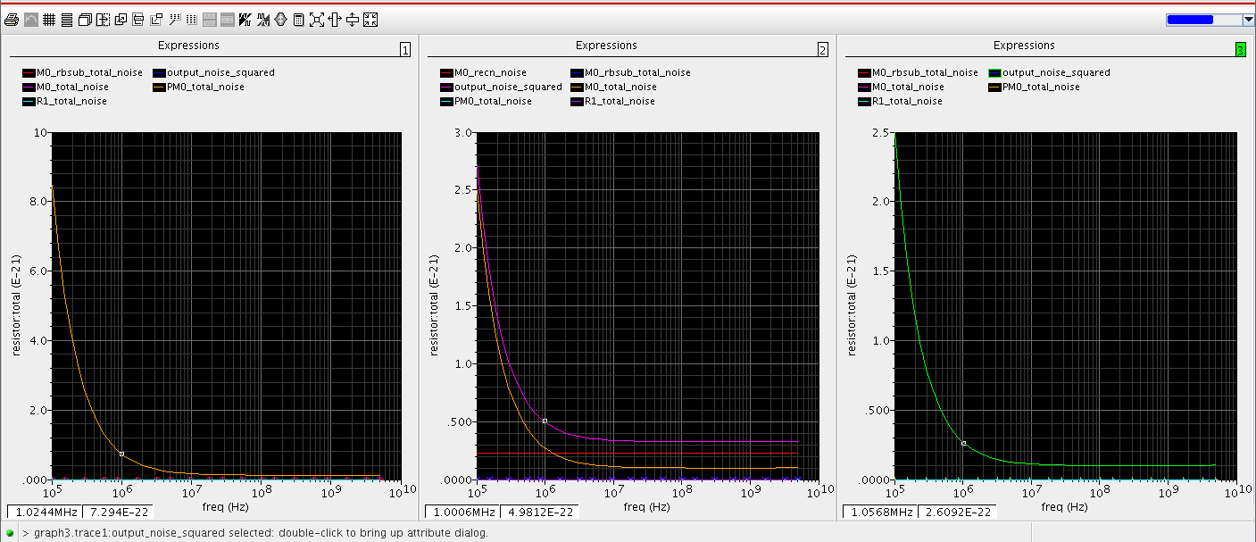
So at 1MHz, the normal pmos has the highest noise, while RF pmos is lower, especially without the noise enhancement (which is even less than theory would predict). At 100kHz, the difference between normal and RF PMOS is even greater.
From what I understand, the normal and RF varieties aren't really different devices (same doping, same oxide, etc), but using the RF device models in my schematic means that when moving to layout I will automatically get cells optimized for noise, which is nice. But when I simulate based on RF models at low-ish frequencies, can my results be trusted?
To further compound the issue, I will actually be biasing the transistors very close to subthreshold, but the model documents say that the RF thermal noise enhancements are not valid for Vgs<0.45V. I have seen that under these conditions, the RF models with noise enhancement actually give much more noise than the normal device models...