Continue to Site

Welcome to EDAboard.com

Welcome to our site! EDAboard.com is an international Electronics Discussion Forum focused on EDA software, circuits, schematics, books, theory, papers, asic, pld, 8051, DSP, Network, RF, Analog Design, PCB, Service Manuals... and a whole lot more! To participate you need to register. Registration is free. Click here to register now.

Altium: how to create schematic pins that have multiple physical pads?

Status
Not open for further replies.

tinkerer_guy

Newbie level 5
Joined
Oct 17, 2015
Messages
8
Helped
0
Reputation
0
Reaction score
0
Trophy points
1
Activity points
96
Hi,

I want to create a part in Altium that has multiple, standard packages (QFN-20 and 16-pin WCSP). Some high-current schematic pins have more than one physical pad connected to them. Moreover, it's different for the two packages - the 20 pin package has more "repetitions" of the high-current pins. I am wondering which approach to take when building the part. every solution I see has drawbacks:

1. I can place multiple schematic pins so that each physical pad is represented uniquely. Besides being "ugly" on the schematic, it requires building a different schematic symbol for each packagem since the pin repetitions are different. Clearly this is not a good option.

2. I can do the same as above but with some pins hidden and underneath the visible pins with the same purpose. while this is no longer visibly ugly, the problem of creating a different part for every package still exists.

3. I can modify each package footprint (in the PCB library editor) so that repeated function pins have the same pin number. it's actually demonstrated in this Altium PDF with a TO3 footprint (see page 47). both pins connected to its metal body are numbered "pin 3". However, this means I need to copy the standard QFN and WCSP footprints and modify them just for this specific part. this doesn't look like the most modular approach (for example, say I want to change to a QFN package with longer pads for better access, I have to manually redo the pin assignments). It also doesn't sound right to have a QFN package with four "pin 7"s scattered around it instead of the sequential pin numbers one would expect.

Can you suggest a better approach than the above? Or, if you use one of these approaches, how do you handle the drawbacks I mentioned?

thanks!
Guy.
 

no one, then...?

maybe my post was too long. I'll summarize:

what's a good way to build a part with more than one package, where each package has multiple pads for some pins (but not the same qty in each package)? my post above details some options, with drawbacks for each one. I have yet to find the "proper" way to do that.

help anyone?

thanks,
Guy.
 

Have you got a picture of what the pinout should be?

Or even type in the pin to pin connectivity from each package.

In CADSTAR (I don't do Altium) we would add pins for both packages and those that need to be connected together with a single pin on the schematic would be connected with component copper.
I don't know if Altium can do this.

Either way, it's a real oddball and is likely to look ugly.... :)
 

I don't know if Altium has specific limitations in this regard (I guess not), but having different pin mappings respectively different parts for different packages is the regular way to handle the problem. It's usual to show the actual pin mapping in the schematic.

When you place a component with multiple pads representing a logical pin, the intended connection is shown as airline and has to be routed like other connections.
 

thanks for the replies. Indeed, if Altium had pin mapping that supports one schematic pins to multiple footprint pads, this would have been the perfect solution to this problem. However, I didn't find a way to do that (anyone knows differently?). The pin mapping feature I'm aware of in Altium is strictly one-to-one.

in this discussion here a while ago, someone asked a similar question. The advice given to him is to build a footprint with multiple pads that have the same pin number. I don't want to go that route since I am using standard footprints (QFN etc) and it would be awkward, see option #3 and its drawbacks in my original post.
 

O.K., apparently I was wrong when expecting industry standard features with Altium Designer. I was only occasionally using the tools at a customers site and am not really familiar with it.

Perhaps an Altium power user can confirm that there's actually no single schematic pin to multiple footprint pads mapping feature provided?
 

What industry standard?

There are no industry standards when it comes to PCB CAD packages. ;)
 

O.K., industry standard isn't the right term. But a component definition with symbol to footprint mapping is provided by most cad packages. Racal Redac's Redcad (the later Cadstar) already had it more than 30 years ago.
 

Cadstar only currently maps one pin to one pin, has never mapped one schematic pin to many PCB pins, that feature is coming soon....
This is a feature I have been wanting for years so that thermal vias in power pads can be catered for.
In Cadstar you can connect pins in the footprint using component copper, which does get round the problem.
Redboard was the PCB package, Redcad the schematic capture... a big Improvement over drawing manual schematics and creating manual netlists... I remember there was pin limit per symbols and footprints in the early days, some CPUs had to be done as two or more symbols and matching footprints. Ah the good old days, I remember being an optimistic 24 year old in 1985 sitting down in from of my Swann monitor (a fish bowl) and booting up the cad programs... also used AutoCAD, nothing much has changed really... still sat in front of two monitors now, just no optimism left.....:-D:-D
 

My remembrance seems to fool me regarding Cadstar features. I must confess that I didn't use Cadstar after year 2000. Thank you for clarifying. But Redcad is in fact the package name, Redlog and Redboard are the schematics and layout tools, I reviewed the 1986 manual.

Mentor Integra Station (originally Spea TopCad) had definitely the mapping feature and Pulsonix adopted it.
 

Thanks Mattylad, I actually linked to this Altium document (in its PDF version) in my original post so I am aware of this option. my problem with it is that I want to use standard packages. it sounds wrong to have a QFN-20 footrprint modified just for this part to have, say, three "pin 7"s and no pin 8 or pin 9. It will confuse whoever looks at the schematic for pin numbers when debugging the board, will make this completely non-modular, and generally a mess. let's say I want to replace my QFN footrprints with ones with longer pads, to allow easier hand rework or debugging. I have to redo this package, since it's not a standard QFN-20 from a standard library but this custom Frankenstein with all its pin numbers messed up...
 

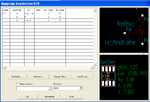
That's how the part pin mapping looks in Integra Station:

Integra pin mapping.png

Simply assign multiple pads to a schematic pin.
 

It's an oddball, the schematic will not look the best - you can only do what you can do to make it.
 

I would use one symbol per IC anything clever tends to cause mistakes or problems later on, keep it simple where possible.

Yes I am old Mathew and feel it at the moment:-(
 

Status
Not open for further replies.

Part and Inventory Search

Welcome to EDABoard.com

Sponsor

Back
Top