wr233608
Newbie level 1
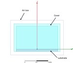
I have a simulation model in HFSS that consists of a printed dipole antenna on a substrate but enclosed with a cover ( ceramic material). Such a model is to emulate an antenna inside of a chip.
I am not sure whether to place the radiation boundary at the outer faces of the cover or create an air box surrounding the model and place the radiation boundary on the faces of that air box.
I would really appreciate your input and feedback.
Attached is a a cross section of the model.
Thanks!
I am not sure whether to place the radiation boundary at the outer faces of the cover or create an air box surrounding the model and place the radiation boundary on the faces of that air box.
I would really appreciate your input and feedback.
Attached is a a cross section of the model.
Thanks!