Continue to Site

Welcome to EDAboard.com

Welcome to our site! EDAboard.com is an international Electronics Discussion Forum focused on EDA software, circuits, schematics, books, theory, papers, asic, pld, 8051, DSP, Network, RF, Analog Design, PCB, Service Manuals... and a whole lot more! To participate you need to register. Registration is free. Click here to register now.

SPI on FPGA - output 1 byte from one port?

Status
Not open for further replies.
I tried testing it after changing the state of CS in the code. I then plugged it onto an oscilloscope, to see if the system also performed as I hoped it would do.. But from what i can read from the oscilloscope, The MOSI starts sending out a high bit, rather than sending 7 low bit and then 1 high. It looks like it is reversed?..

About
Code:
shift_reg <= shift_reg(shift_reg'left -1 downto 0) & '0';

My plan was initially to shift each bit using this method, I was at that time confused on i should tell it to only do it, 7 time, or 10 times when i have to read data, and how exactly that operator worked.
 

You really need to create yourself a testbench, to make sure everything worked as you expect it to in the simulator, so you dont have to spend time debugging in hardware.
 

I tried testing it after changing the state of CS in the code. I then plugged it onto an oscilloscope, to see if the system also performed as I hoped it would do.. But from what i can read from the oscilloscope, The MOSI starts sending out a high bit, rather than sending 7 low bit and then 1 high. It looks like it is reversed?..

About
Code:
shift_reg <= shift_reg(shift_reg'left -1 downto 0) & '0';

My plan was initially to shift each bit using this method, I was at that time confused on i should tell it to only do it, 7 time, or 10 times when i have to read data, and how exactly that operator worked.

If you want to shift from MSB to LSB then just swap the position of the '0' and change the range.
Code:
shift_reg <= '0' & shift_reg(shift_reg'left downto 1);
 

I tried to fix some issue with the simulator, and do get an output which looks more reasonable than before..

But there is one thing, I don't understand with with the output i receive from the ADC.

My input to the ADC is at the moment V_ref => which means that the output of the ADC after the init sequence "000000011000" should be "1111111111", as long CS is low.

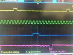
Problem is though, when i tested with the scope, I noticed that the output of the ADC is still high even when CS is high?.. should it not reset when it goes high?

IMG_3885.JPG

(Yellow line being CS)
(Green line being CLK to ADC)
(Blue being MOSI)
(Magneta being output from ADC)..

It does appear like the ADC notice when CS goes high, as the output from the ADC begins to jitter a bit, but it's logical high.. which makes no sense to me..


Here is the updated code:

Code:
library IEEE;
use IEEE.STD_LOGIC_1164.ALL;
use IEEE.numeric_std.all;
use IEEE.STD_LOGIC_ARITH.all;
use IEEE.STD_logic_unsigned.all;
use ieee.numeric_std.all;


-- Uncomment the following library declaration if using
-- arithmetic functions with Signed or Unsigned values
--use IEEE.NUMERIC_STD.ALL;

-- Uncomment the following library declaration if instantiating
-- any Xilinx primitives in this code.
--library UNISIM;
--use UNISIM.VComponents.all;

entity main is
    Port ( MISO : in STD_LOGIC;
           MOSI : out STD_LOGIC;
           CS : out STD_LOGIC;
           SCLK : out STD_LOGIC;
           CLK : in STD_LOGIC;
           debug_led: out std_logic_vector(9 downto 0)
           --debug_TX: out std_logic_vector(23 downto 0)
           );
end main;

architecture Behavioral of main is
--signal prescaler : integer range 0 to 3500000 := 3500000 ;
constant N : integer := 11;
signal prescaler_counter : integer range 0 to 50000000 := 0;
signal newClock : std_logic := '0';
signal TX :std_logic_vector(N downto 0) := "000000011000";
--signal TX :std_logic_vector(11 downto 0) := "000000011000";
signal RX : std_logic_vector(9 downto 0) := "0000000000";
type state_type is (start,state2,state3,state4,state5,state6);  --type of state machine.
type TXRX  is (waiting, working); 
signal state : state_type := start;
signal shift_counter: integer range 0 to 23:= 13;
signal init_tx: TXRX := waiting;
signal init_rx: TXRX := waiting;
begin

prescaler01: process(clk, newClock)
begin
    if rising_edge(clk) then 
        if prescaler_counter < 60 then
            prescaler_counter <= prescaler_counter + 1;
        else
            newClock <= not newClock;
            prescaler_counter <= 0;
       end if;
    end if;            
end process;

SCLK <= newClock;

-- FPGA transmit data on falling_edge
-- FPGA reads data on rising_edge


SPI_state: process(newClock)
begin
   if rising_edge(newClock) then       
        case state is   
            when start =>
            debug_led <= "0000000001";
                CS <= '1';
                MOSI <= '0';  
            state <= state2;
            when state2 => -- Send init bits. 
                debug_led <= "0000000010";
                CS <= '0';
                shift_counter <= shift_counter - 1;
                TX <= TX(N-1 downto 0) & TX(N); 
                MOSI <= TX(N);
                if shift_counter = 0 then 
                   MOSI <= '0';
                   shift_counter<= N;
                   state <= state3;
                end if;
            when state3 =>
                debug_led <= "0000000100";
                CS <= '0';              -- Sample/hold
                state <= state4; 
            when state4=>
                debug_led <= "0000001000";
                CS <= '0';              -- Sample/hold
                state <= state5; 
            when state5=>
                debug_led <= "0000001000";
                CS <= '0';              -- Sample/hold
                state <= state6; 
            when state6=>
                 debug_led <= "0000001000";
                 CS <= '0';              -- Sample/hold
                 state <= start; 
            when others =>                 
                debug_led <= "1111111111";                   
                state <= start;           
        end case;
    end if;  
end process;
end Behavioral;
 

SPI transfers use opposite edges to transmit and receive, both control signals and data. So why are both the MOSI transitions occurring coincident with the rising edge of the ADC clock?

The ADC is obviously transmitting on the falling edge of the clock therefore it will be sampling the MOSI and the CS on the rising edge of the clock, which means you are changing those inputs at the same time they are being sampled.

The code you show also has no falling edge clocking for the outputs.
 

well.. I tried clocking data out on the falling_edge, I still got the same result..
I have an 10 bit delay (10 rising edges) to ensure i read the data before i change the CS to high.. But still..I don't get why the ADC output doesn't become zero as CS goes high...

- - - Updated - - -

if i put the frequency down to 41.7 kHz I can clearly see that the output of the ADC goes towards, until the init bit has been recognized, at which it start outputting the null, and the 10 bits. It seems like the time I set not high enough.

But it doesn't make sense that i have to wait that much time, until the output becomes zero..
 
Last edited:

You never stated what your clock frequencies are. What frequency is your input clock CLK? Based on your latest observation are you sure you've followed all the timing parameters in the datasheet? Increasing the clock period and it starts working typically means you've violated some timing parameter.

Also what voltage are you using, running the ADC at the lower voltage means you have to run the ADC a lot slower.
 

The clock i am using it 3.57 Mhz
ADC V_ref = V_dd = 3.3V

I should be be within the constraint which is set by the Datasheet.


At the lower rate I could clearly see that it went towards zero.. It has the same characteristics of an capacitor being discharged, which is also visible if i increase the time of which the CS is high.
 
Last edited:

The datasheet shows that the maximum clock rate to the ADC (a.k.a. newClock) to be 3.6 MHz with a 5V supply. You aren't powering the ADC with 5V so you won't be able to use it at the maximum clock rate.

Typically the performance and voltage aren't exactly linear so you'll have to include some margin when using a voltage between 5V and 2.7V. If it was linear (which it's not) then the maximum frequency you could run it at would be ~1.94 MHz. I would probably run it below 1.7 MHz to be safe.

Are you sure you have the right frequency? Taking newClock (3.57 MHz) and multiplying it by 61 gives 217.77 MHz, which seems like a highly unlikely frequency.
 

You aren't powering the ADC with 5V so you won't be able to use it at the maximum clock rate.

Something you could reference to?

Are you sure you have the right frequency? Taking newClock (3.57 MHz) and multiplying it by 61 gives 217.77 MHz, which seems like a highly unlikely frequency.

I am using a 50 mhz, I used 60 to test it, but yeah.. If I only count up to 6 will it become a 3.57 Mhz clock from a 50 MHz

- - - Updated - - -

and what about the out has to be read using RC filter?
Could that have something to do with it?
 

You aren't powering the ADC with 5V so you won't be able to use it at the maximum clock rate.
Something you could reference to?
From page-3 of the datasheet
**broken link removed**

I am using a 50 mhz, I used 60 to test it, but yeah.. If I only count up to 6 will it become a 3.57 Mhz clock from a 50 MHz
You better learn how to count in VHDL.

Code VHDL - [expand]
1
2
3
4
5
6
7
8
9
10
11
prescaler01: process(clk, newClock)
begin
    if rising_edge(clk) then
        if prescaler_counter <= 6 then
            prescaler_counter <= prescaler_counter + 1;
        else
            newClock <= not newClock;
            prescaler_counter <= 0;
       end if;
    end if;            
end process;


That code counts from 0-7 (i.e. 8 counts) not 6. The <= 6 makes it increment when 6 so it goes to 7, then it rolls back to 0 when it takes the else branch.

The standard method is always

Code VHDL - [expand]
1
2
3
4
5
if count < PERIOD-1 then -- so if we want a period of 6: then 4<5 increments and 5<5 resets count to 0.
  count <= count + 1;
else
  count <= 0;
end if;


which is why just like Tricky said why don't you create a testbench and run a simulation before trying it out in hardware. If you had done that you would have noticed the count errors.

and what about the out has to be read using RC filter?
Could that have something to do with it?
Huh? out? the part only has a Dout and that is a DIGITAL output, which is driven by the SPI output shift register. You said you were using this part.

- - - Updated - - -

BTW, your waveform does not match the number of clocks between CS pulses in the datasheet, you have a period of 17 clock cycles and the datasheet shows 18. You probably also have the bit alignment shifted for the MOSI. Run a simulation of the circuit instead of looking at scope traces, with nearly static values. Write a BFM for the ADC and generate random values for the data to be output.

Your MOSI line is going high when it's supposed to be a don't care in the timing diagram in the datasheet.
 

So I've scaled the newClock down to 1.79 Mhz. I am able to output a binary value on to my LED, but as you just have mentioned, it not the right value. Which might be due to the timing as you mention.

To be sure i not sure how the posted code was able to synthesize, due to the size of the constant N, but I am now only shifting it 12 (N = 11) times.

Those 17 clocks you mentions is including the Data output from the ADC, which wasn't included in the previous code, which I've added now

So after init sequence has been performed using 12 clocks => "000000011000".

Code:
when state3 =>
                debug_TX <= "00000100";
                CS <= '0';              -- Sample/hold
                state <= state5; 
            when state4=>
                 debug_TX <= "00001000";
                CS <= '0';              -- Sample/hold     Analog sample  imput time = 1.5 clock (10th bit = null)
                state <= state5; 
            when state5=>
               debug_TX <= "00010000";
               CS <= '0';              -- Read
               shift_counter <= shift_counter - 1;
                RX <= RX(8 downto 0) & MISO;
                if shift_counter = 0 then
                    debug_led <= RX; 
                    MOSI <= '0';
                    shift_counter<= N;
                    state <= start;
                end if;

Which i from counting the clocks between CS high and high (in simulation) can see contains 24 clocks.. So 7 extra clocks.
 
Last edited:

So my final solution end up looking like this.

Code:
SPI_state: process(newClock)
begin
   if falling_edge(newClock) then      
        case state is   
            when start =>
                debug_TX <= "00000001";
                CS <= '1';
                MOSI <= '0';
                RX <= "0000000000";
            state <= state2;
            when state2 => -- Send init bits. 
                CS <= '0';
                shift_counter <= shift_counter - 1;
                TX <= TX(N-1 downto 0) & TX(N); 
                MOSI <= TX(N);
                if shift_counter = 0 then 
                   MOSI <= '0';
                   shift_counter<= 10;
                   state <= state3;
                end if;
            when state3 =>
                MOSI <= '0';
                CS <= '0';              -- Last bit init bit;
                state <= state4; 
            when state4=>
                CS <= '0';              --T_sample from falling - falling
                state <= state6; 
            when state6=>
               CS <= '0';              -- Read
               shift_counter <= shift_counter - 1;
                RX <=  RX(8 downto 0) & MISO;
                if shift_counter = 0 then
                    MOSI <= '0';
                    shift_counter<= N;
                    state <= start;
                end if;
            when others =>    
                state <= start;           
        end case;
    end if;  
end process;

It seem to be working.. eventhough the timing (in simulation) seems a bit off, Which also can be seen from by looking at the scope, CS and the Dout doesn't seem to change uniformly for each time it reads a new value.
 

I don't think extra clocks are a problem, that just means you will be sampling at less than the maximum rate for a given clock frequency. As long as the CS period remains above the minimum of the effective clock rate of 10 KHz you should be fine.

In SPI you are supposed to capture the MISO on the RISING EDGE not the falling edge. For instance you would make your FSM operate in the rising_edge domain and then the outputs of that FSM would be clocked out of the FPGA using a falling_edge register.

Fortunately in this case the Dout of the SPI slave has between 125-200 ns Tco. So the minimum value for best case PVT will still be quite large.
 

The problem i not able to determine the frequcy as is occurs at different time on the clock, and not with a fixed distance..
 

The problem i not able to determine the frequcy as is occurs at different time on the clock, and not with a fixed distance..

The problem is that I am not able to determine the frequency of the CS, as it doesn't seem operate with an constant period.
 

CS is not a periodic signal. It is used to determine when the bus is active. It is asserted when data is transfered and de-asserted when there is no data being transfered. This enoughs the slave to disable it's registers and save power.
 

How would i determine whether my output is correct or not..

I could measure the output channel, but i keeps changing as cs goes from high to low.. measuring that won't anything useful.. looking at the scope.. CS high and low state aren't the same, even though count clock events.. So i am not sure whether the output can be read clearly from that.
 

It looks fine on the TB, but how do i check it hardware wise..

I added some LED on to 10 port which were suppose to show the binary value, but as it keeps tuning on and of, I am not sure whether it shows the right binary value.
 

Status
Not open for further replies.

Part and Inventory Search

Welcome to EDABoard.com

Sponsor

Back
Top