Continue to Site

Welcome to EDAboard.com

Welcome to our site! EDAboard.com is an international Electronics Discussion Forum focused on EDA software, circuits, schematics, books, theory, papers, asic, pld, 8051, DSP, Network, RF, Analog Design, PCB, Service Manuals... and a whole lot more! To participate you need to register. Registration is free. Click here to register now.

[SOLVED] How to configure op amp to produce a 0 to neg 10V swing from a 1Vpp pos signal

Status
Not open for further replies.

designteam

Junior Member level 1
Joined
Oct 1, 2015
Messages
19
Helped
0
Reputation
0
Reaction score
0
Trophy points
1
Activity points
246
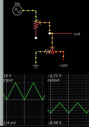
I have a 1Vpp 1Hz repetitive arbitrary wave signal that resides entirely above the DC line. IOW there is no negative-going excursion. This is output from an LM358 inverting op amp buffer powered between +12VDC and ground (0V) rails.

I would like to feed this into an LM358 op amp with a gain of 10 that is powered in a non-standard way as follows. Its "positive" rail is set at 0V. The "ground" rail is set at -12VDC. There is a reason for this, and I do not want to change it.

When I connect the signal from the positively powered buffer op amp to the negatively powered gain stage op amp there is no output, presumably due to the DC level mismatch.

I have seen circuits that shift signals to a higher positive DC level, but not any that shift a positive signal into a negative region. Some level shift circuits also include a capacitor in the signal path, which I would prefer to avoid due to fidelity issues at such a low frequency.

Can someone please provide a working circuit that will enable the gain amp to output the arb wave signal so that it swings between about -10 and 0V? A trimmer adjustment for the DC shift would also be helpful in case I decide to use reduced gain.

This has been a persistent design issue which, due to my limited knowledge, I have not solved so far, either by inquiring online or hours on the bench. Any assistance to get me over this hurdle would be greatly appreciated.

dc_offset_amps.jpg
 

Any op amp can only handle an input voltage which is within its supply rails. Therefore you must condition your input signal so it is in the negative polarity, to be accepted by U2.

A potentiometer can be used to pull the positive signal into the negative region.

- - - Updated - - -


- - - Updated - - -

Tentative values for the potentiometers might be a few k ohms.
 

Brad is right, the supply rails must be far enough apart to cover both max possible input voltage range, and max needed output voltage swing.

To cover that, you will need to power your LM358 from +12v and -12v (24v total across the chip).
Then its a case of adding some resistors and some feedback.
A summing amplifier is called for here.

Ground the +ve non inverting input to 0v.
One resistor maybe 10K between the signal source and the -ve inverting input.
One resistor maybe 100K between the output and the same -ve inverting input.

That will give you a gain of x10 and invert the signal.
0v in, 0v out.
+0.5v in, -5v out.
+1v in, -10v out.

If you want to dc shift the signal, a third resistor (try 100K) can be connected to the same -ve inverting input summing point, and connected to a dc voltage source, depending which way you want to shift the output.
A potentiometer between 0v and -12v supplying the third resistor should give you all the dc shift range you need.

- - - Updated - - -

Here is a schematic:
 

Attachments

  • summingamp.jpeg
    summingamp.jpeg
    27.6 KB · Views: 54

Thanks for the responses so far. This looks like the solution I was looking for.

I have redrawn the circuit based on my understanding of what has been suggested, and plan to try it tomorrow on the bench.

dc_offset_amps_v2.jpg
 

Your new circuit is wrong.
The "buffer" is inverting and has a voltage gain of about 200,000 so it is not a buffer. Its input should be the (+) input and its (-) input should be connected to its output for feedback.
 

Yup, the buffer is all wrong which is why I did not include it in my reply, which on reflection I should have.

That is a separate issue which we need to look at next.

Modify your circuit exactly as Audioguru suggests, and it should all then be sweet.
 

I posted a reply this morning but it has not yet appeared, so I will try again. My apologies if it doubles up.

My thought was to use an inverting buffer since the gain amp is also inverting. Then the output would be in phase with the 1Vpp original signal.

However, I received advice that an inverting buffer would clamp to the 0V rail. I suspect this is what Audioguru was referring to in his post. So I will verify this on the bench. In the meantime, I have left that part of the schematic "as is" until I understand for myself why this could occur.

Here is a diagram that shows the way the above circuit is intended to work within the completed device. The wide area output coils are intended generate a 1Hz uniform field for magnetic testing.

Any further comments much appreciated.

dc_offset_amps_v3.jpg
 

Your "buffer" has its output connected to the signal source. The output is FIGHTING the signal source so it WILL NOT WORK.
Please learn about how to make an opamp an inverting amplifier that uses two resistors: an input resistor and a negative feedback resistor.

The opamp at the top that drives the transistor will not work because it is inverting and its (+) reference input is at ground. Then any positive voltage at the (-) input will cause its output to go to ground and the output will always be close to ground and the transistor it drives will always be turned off.

The transistor at the bottom will be destroyed when it is turned off because its emitter-base will have avalanche breakdown (usually when it has a reverse-bias of more than 5V).
 

Hi,

Look for an RR out Opamp with common mode input voltage range including upper supply rail.
Then configure it as simple inverting Opamp with gain -10.
In+ to GND.

Klaus
 

It might be possible if you can use a RRIO opamp in place of the 358. I won't draw a picture (no graphic sw on this computer), so bear with me.

Positive supply line to ground.
Negative supply line to -12V.
Non-inverting input to ground.
Signal to inverting input through a 1k resistor.
A 10k resistor from output to inverting input.

What happens is that the opamp will strive to keep the inverting input at the same potential as the non-inverting input, ground in this case. Since there's a 1:10 ratio between the resistors the output will be 10 times the input to achieve this balance (Uin/Rin + Uo/Rout = 0).

Since both input and output may go to ground potential a RRIO amp is needed. If the input goes below ground the output stays at zero (no positive supply).

The resistor values are suggestions, you can fiddle them as you please, keeping the ratio. The ratio doesn't take into account the finite gain of the amp, recalculate to the needed precision.
 

I have corrected my mistake with the inverting buffer U1 and added a bit more gain to the second op amp U2 with a 220K feedback resistor. Pin 8 of U2 remains connected to ground. I tested the circuit on the bench and it works well. 1Vpp in and a maximum output swing of -1V to -9V. The 10K pot correctly adjusts the DC level of the output signal from within about -1V from the 0V ground rail until it clips against the -12V rail. I did not have an RRIO amp on hand, so I stuck with the LM358. See diagram this post.

I would like to add a positively powered "mirror image" of the negatively powered amp, and add a transistor follower to each stage to drive the coils as shown in my prior (incorrect) schematic. However, I now consider my original question here solved. Thanks to all who responded.

Later this week, I will work on the issues raised with the positive op amp and negative transistor in my prior schematic. If I can't make it happen, I may start another thread related to that specific part of the circuit. This is a great forum and I am learning a lot.

dc_offset_amps_v4.jpg
 

The (+) input pin 3 of the LM358 does not work when it is within 1.5V from its positive supply pin 8 (Input Common Mode Voltage Range on the datasheet) and you have them connected together to avoid destroying the output transistor.
The schematic of the LM358 on the datasheet shows that each input is a PNP darlington that turns off completely and does nothing if its voltage is within 1.5V from the positive supply.
 

Thank you for pointing that out, but the circuit does work as drawn in my most recent diagram, and was verified on my scope. In fact, I noticed it even works when pin 3 of U2 is not connected to anything. So there must be something else going on other than what you suggested. Perhaps your statement would apply to a more conventional design.
 

Status
Not open for further replies.

Part and Inventory Search

Welcome to EDABoard.com

Sponsor

Back
Top