Continue to Site

Welcome to EDAboard.com

Welcome to our site! EDAboard.com is an international Electronics Discussion Forum focused on EDA software, circuits, schematics, books, theory, papers, asic, pld, 8051, DSP, Network, RF, Analog Design, PCB, Service Manuals... and a whole lot more! To participate you need to register. Registration is free. Click here to register now.

[SOLVED] How does an hFE tester work?

Status
Not open for further replies.

d123

Advanced Member level 5
Joined
Jun 7, 2015
Messages
2,505
Helped
494
Reputation
992
Reaction score
525
Trophy points
1,393
Location
Spain
Activity points
27,148
Hi,

I have been looking at simple BJT hFE tester circuits, and reading up on them a bit. What I wanted to specifically check is:

a) To make a rudimentary hFE tester to sort a few NPN and PNP BJTs into gain batches (70 - 80, 80 - 90, 90 - 100, etc.).
Is the main point to inject a constant current (100uA, 1mA, etc.) into the base of the DUT, and - for example - measure the voltage across a shunt resistor?

b) Is the matter of also testing for leakage of great importance for the above purpose, or for my basic requirement (approximate gain measurement and classification) can I skip that part of the circuit?
I ask as not that many of the schematics I've seen include this feature.

c) I have limited knowledge of biasing transistors, but from what I've read so far on hFE testers the topic gets scant comment, so have a doubt as to whether I also need to bias the base voltage.
Would I need to set the Vbe voltage, or is the base current all that matters for this circuit?

Thanks.
 

The current gain of a transistor changes when its temperature changes so the test is done with a short duration pulse so it does not heat up. The datasheet tells you the width of the pulse and its duty cycle.
The current gain of a transistor changes when its collector current is changed.
The base-emitter voltage of a transistor also changes when its temperature changes but the Vbe is not used top test the current gain.

Make a constant current source and pulse it into the base. Measure the collector current pulses to determine the current gain.
The currents should be much higher than any leakage current that can be ignored.
 
  • Like
Reactions: d123

    d123

    Points: 2
    Helpful Answer Positive Rating
Most simple Hfe tester work by injecting a small current into the base, the measuring the collector current. Better ones do that then null the current measurement before injecting a slightly higher base current and measuring the collector current again. The difference in current as the base current increases is then used to calculate the gain.
Hfe = delta Ic / delta Ib.

For most silicon transistors, the leakage 'Icbo' is very small and unless you need very accurate checking, can be ignored.

Brian.
 
  • Like
Reactions: d123

    d123

    Points: 2
    Helpful Answer Positive Rating
Hi,

I recommend to read some datasheets.

As an example I opened NXP_PHILIPS BC850 datasheet.

Now look where hfe is specified.
It is specified at two operating points: 10uA and 2mA. Vcc is 5V.
This says a lot. The only thing you need to adjust Ib to get the desired Ic. Now divide Ic/Ib to get hfe.

Instead of adjusting Ib manually you could use an Opamp to do this for you.

Klaus
 
  • Like
Reactions: d123

    d123

    Points: 2
    Helpful Answer Positive Rating
Hi,
To make a rudimentary hFE tester to sort a few NPN and PNP BJTs into gain batches (70 - 80, 80 - 90, 90 - 100, etc.).
Measured Hfe depends on all kinds of things, but if you wish to sort and match a batch for a specific application, you want the Hfe's to be the same under the operating conditions the device will be operating in your circuit.

So build your tester to bias the transistor dc current very close to the circuit operating conditions it will be used in.
Then inject a very small known ac current into the base through a series resistor.

You can then measure the ac voltage on the collector, and work out the Hfe by knowing the collector load resistance and ac current swing.

The transistors set dc bias could be set from microamps to amps (for power transistors), but you need to set it up to reflect the actual final operating condition, and keep the amplitudes as low as can be conveniently measurable to the required accuracy.
 
  • Like
Reactions: d123

    d123

    Points: 2
    Helpful Answer Positive Rating
hFE is DC current gain. hfe is AC current gain at one frequency.
The first post asked about hFE, not hfe. No frequency was mentioned.
 

Thanks very much to you all for your explanations and the suggestions, your replies have helped to clear up the things I was unsure of, drawn my attention to things I've read and re-read in datasheets for the last months and have never really thought of much or understand perhaps (beyond looking at max. operating characteristics, hFE 35 - 300 and so on), and have provided additional useful information which will help a lot with having a first go at the circuit.
Thanks ever so much.
 

The TEXT in a transistor datasheet guarantees its Vbe and hFE minimum, typical and maximum spec's since each transistor even with the same part number is different. The GRAPHS in a datasheet shows only its typical, usually not its minimum and not its maximum spec's. When you buy a transistor you will not know if it has minimum, typical or maximum spec 's so its circuit should be designed so that any of them work well.
 

hFE and leakage is useful when biasing is weak without negative feedback to regulate independent of these parameters.

It is somewhat related to Vce(sat) for a given Ic/Ib ratio which is usually rated at 10:1 and in rare cases up to 50:1

However hFE varies with Ic and peaks well above low operating range for Ic, so often 10mA to 100mA are used, more if pulse S&H reading.

For portable 9V instruments, only low current is tested but Vce is fixed to something like 2V then fixed base current applied and Ic current sense is amplified to read output current ratio from known input current.

Lowest power way is 5.6V zener biased base voltage with 500k trimmed Re to get 5V/0.5M= 10 uA CC source & sink and measure current of Ic for hFE gain up to 1000 on 10mA scale.

But this is no good for power transistors, so CC range switches are needed, and in some cases one shot high current pulse testers are designed.

So it depends on your needs. Accuracy over a wide range of Idc or simplicity with poor range.

- - - Updated - - -

ref
https://www.google.ca/search?q=hfe+...ehsD2A&biw=1132&bih=649#imgrc=0196YdcSPldBeM:
 

Hi, what I meant was that when I've read/gone through datasheets - this also goes for ICs - the test circuits they show, or the notes below the specifications that refer to pulse duration and duty cycle, are both aspects that I assumed were more for professionals/companies to use, if you understand what I mean, I hope, but now that you've drawn my attention to how useful they can be, thanks.

Trying to absorb everybody's comments/knowledge, I'm glad to know that (for what I'm doing) the main points to focus on are base current and a short pulse, and forget about measuring leakage current, and for a better Device take two measurements.

As I don't know the circuits which in the future I will use the transistors in, except for a couple of things I'm doing, so as a consequence nor can I know the operating conditions, I'm just aiming to sort the transistors into rough hFE groups, as I said before, as I know that using a DMM hFE tester (before I damaged the tester/it broke in April) transistors in the same batch ranged from 70 to 120, but appreciate your point about designing the circuit to fit them all, but add that for some calculations it helps to know if I'm using something with a supposed gain of 70 or of 120, to save at least a little bit of time later when the sums don't match reality (e.g. basing them on an hFE approx. 95) and - in my case - have to tweak resistor values, for example.

I have a first version schematic, which I know needs a few more changes before it's right, while I'm thinking through the design stage and doing calculations. I see that I seem to need to use 100uA + 1 Ohm shunt, or 1mA + 100 milliOhm shunt; but have doubts that also adding 10uA + a 10 Ohm shunt would be that useful.

And separately, referring to power transistors, I'd hoped to use the 10uA base current as I wanted to keep the collector currents as low as possible because of power dissipation in the devices themselves and hoping to avoid having to add a heatsink or high wattage shunt resistors; however, I read some won't turn on without 10mA or even 100mA base current - is this so?
This puts me off a bit as one or two darlingtons I have supposedly have a gain of about 3500 - 0.01A x 3500 = 35A...it's just not going to happen if that is true, which is why I wanted to use 10uA: 0.00001A x 3500 = 0.035A, or even the 100uA base current which is only 0.35A/350mA. Is there some way around this? I imagine not.

- - - Updated - - -

From what I've read and understood of everyone's advice and comments, which are all helpful and enlightening, to summarise one aspect: it seems to me - perhaps I'm mistaken - simple hFE testers (like, and especially, the DMM I had which had that feature), such as the one I hope to learn things from making and use for practical purposes, produce what could be described as a somewhat arbitrary and in a sense meaningless number which gives a kind of guesstimate of the actual gain/beta/hFE of a device, but which will be different in a real circuit depending on how it is actually used, so at best the simple "testers" might show how much difference there is between two identical looking BJTs under one single condition. Hmmm...
 

Your 'updated' understanding is correct. Measuring gain with one model of DMM may give a completely different reading to another model. For purposes of confirming the transistor is functional and for comparing transistors if you need matching gains, they are adequate.

Brian.
 

That is the problem....

We are trying to measure the slope of a curve at one particular point on the curve.
Its not possible to just assume that the slope is equal to a straight line drawn between the point of interest, and origin.

Its why I suggested earlier in #5 to use a low amplitude (low frequency) ac method of measurement to measure dc gain.

Back in ancient times, some people used curve tracers to measure and compare transistor characteristics. These were sold as commercial instruments.
These sweep through the whole range and plot a series of curves on the screen of an oscilloscope, similar to what you see on a data sheet.
This was before the age of computers.
It would be possible to do something similar today in a much nicer way with some software and a PC.
You could even overlay multiple sets of curves and match transistor characteristics with extreme precision.
 
Last edited:
  • Like
Reactions: d123

    d123

    Points: 2
    Helpful Answer Positive Rating
The OP (d123) suggests they are looking for generic methods of testing rather than at the voltage/current encountered in a specific application. A DMM with transistor test will verify the device has gain and is therefore functional and can be used to compare different transistors, for example to match their gain, using it's own measurment conditions.

For full testing in real application conditions, it would be best to simulate the operating environment although the same basic method of measuring collector current change for a known change in base current still applies.

Thinking about it, I don't recall seeing any general purpose 'plug and play' transistor testers that can plot curves under different operating conditions that work with a standard PC, at least at affordable prices. I'll have to put my inventing hat on and get busy!

Brian.
 

Thinking about it, I don't recall seeing any general purpose 'plug and play' transistor testers that can plot curves under different operating conditions that work with a standard PC, at least at affordable prices.
Brian.
This sort of thing rather died out with the introduction of low cost mass produced op amps.
Nobody today gets a handful of plastic transistors and tries to design an opamp from scratch to serve some ultra precision purpose.
Even duplicating the humble and ancient 741 in discretes might be a real mission.
But in the old pre op amp days that was the only choice available.
Either that, or build it using valves !


Laser trimming and very clever die fabrication techniques have pretty much removed the need for manually matching of discrete transistors to close tolerances.

Here is a Tektronix curve tracer:
Tektronix_577-D2-177.JPG
 
Last edited:

We are missing the circuit where the OP wants to use matched transistors.
Instead of matching, maybe the OP needs to know how to design a transistor circuit so their range of spec's do not affect the performance.
 

The reality that hFE and hfe has a wide range of values.
The spec for hFE typ:min ratio of 5:1 and can be as much as 30:1 max:min or more (over temp) and as low as 2:1 max:min for binned part numbers.

Also hfe reduction usually starts when Vce<2, which is the non-linear cause of THD and compression of peaks in linear operation with feedback. In large signals Vce(sat) is the cause signal clipping.

In the linear AC gain case, hfe, non-linear operation begins whenever Vce approaches Vce=2V and under and should be avoided for high linear operation. For use as a switch (non-linear by def'n) then default standard is spec. Ic/Ib ratio for Vce(sat) or hFE of 10. This is important for estimate Ic(t)*Vce(t)=Pd * duty cycle and heat rise. Also ratios of 20 and/or 50 are used some datasheets ( for special design with very high hFE.) We often use 0.2V for switched voltage under light current which depends on a tradeoff for diode doping that affects the forward bias of each PN junction Vce=Vcb-Vbe. When we want this to =0V, like an ideal switch a special process in the past using gold doping ($) was improved and patented by Diodes Inc (nee XETEX) (but still more $) and this difference approaches xx mV, instead of 200~500mV that we often assume. This characteristic is highly regarded for transistor high current switches with low capacitance and high voltage, but expensive and is also used by Diodes Inc for IGBT's and Mitsubishi, the leaders in big IGBT's which have FET inputs and BJT outputs.

The slope of Vce(sat) vs Ic becomes a linear resistance (* bulk region of PN) such that we call it Rce similar to RdsOn.

A good rule of thumb is the effective estimate of the switched Operating Point for Vce is to follow the datasheet for Vce(sat) at Ic/Ib=10, (20 or 50) as the case may be. the other method is calculate the Rce value and use this like RdsOn or ESR in reactive parts.

The best design practice is to define your limits to error, from all sources ( enviromental range , component tolerances, vendor variations and reduce the effects of expected from hfe variation consider design methods using current sources, mirrors and feedback ratios to determine Quiescient Operating Points. There is no substitute for good design, but when a tight range of hFE is needed, rely on good Japanese sources for transistor part number suffix, where hFE binning is standard to reduce the range to 2:1 typ. for each bin Leaders such as ROHM INC are followed by many others.

Thus hFE testing is needed just for Quality Verification and not good design. Transistor testers can be as cheap as $1 for DC hFE or $100k with Microwave Smith Charts for RF design verification.

For RF, Analog and Switch design, all you should need to define DC operating point is the datasheet.

A rule of thumb I use
for non-linear hFE is to use the Ic/Ib ratio specified for TYP and calculate the Vce(sat)/Ic ratios for variations in Rce and use like ESR for predicting voltage ( and heat) rise with current. This is a good linear approximation a non-linear switch and is identical to the estimation of MOSFET's RdsOn and can be applied to all PN junctions including as I often indicate as ESR of the PN junction.( bulk resistance) This Rs or rBE, rCB and Rce or whatever symbol) is explicitly related to bulk size and power dissipation and thus inversely relates ESR to Pd of the package for any LED, diode, or Vce saturated operating point.

I simplify this linear feature for non-linear operation and simply call it ESR (effective series resistance) which is very effective for designing the DC operating point of transistor switches, diodes and LED's.

I can prove (or at least demonstrate from any datasheet) how ESR* Pd(max) ranges from 0.5 to 1 typ. for any PN junction.
 
Last edited:
  • Like
Reactions: d123

    d123

    Points: 2
    Helpful Answer Positive Rating
We are missing the circuit where the OP wants to use matched transistors.
Instead of matching, maybe the OP needs to know how to design a transistor circuit so their range of spec's do not affect the performance.

Hi all. I'm learning rather a lot from a simple question, which is great, thanks - some things will take a few re-reads to absorb what is being said if I'm honest, but there's nothing wrong with that.
The description of what a curve tracer does is very useful, I've seen a couple of threads with people asking after them and commenting how costly they are, even second-hand :(, now I have some idea of what they are for.
I'm also seeing that in a sense and for well-explained reasons I don't really need to make an "hFE tester" (not that that's going to put me off the venture!), even if it is a worthwhile way of learning more about transistors and making another "lower-end cheapo" measurement device, I also see that "It'll take a week" is more like a month or so at least, which is okay.

Talking about "in ancient times", I nearly got my hands on some TO-100 LM723s recently, but they never arrived and I just got the refund instead, shame as I was really looking forward to them, some other time I hope...

As I said above, I'm going to re-read your posts in this thread every so often as slowly the things I don't understand will sink in or become clearer, and many thanks.

And to give an example of an actual circuit where it doesn't really matter maybe or perhaps not at all, but to go eliminating reasons I would like to see if roughly matching the BJTs anything improves: I'm on my second breadboard version of a 555 using 2N2222As and 2N2907s, and both have worked a few times in monostable mode but then sputter and die. I know there can be lots of "human errors" and other reasons the circuit works erratically or not at all in the end, but as both times it has worked for a while, I'd like to match the transistors (that appear in the comparator part, for exemple). I'm copying the ST SE555 datasheet schematic, which is pretty identical to the Signetics one, and obviously works when not in my hands.

I really appreciate the shared knowledge, it's very interesting and some parts are eye-opening, thanks a lot.
 

You are wasting time trying to make a discrete version of a 555 IC. The transistors in an IC are special because all transistors on the same monolithic chip are identical and you will never know their spec's so trying to use a 2N222A and 2N2907 with their wide ranges of spec's results in way too much current or not nearly enough current.
 

Okay, indirectly your answer about too much current or not enough is a big help.
I see your point, and am aware that an IC is not a handful of off-the-shelf devices, but disagree about it being a waste of time - there seem to be a lot of projects where people make a version of the 555 that work, and it's a way of doing something a bit more interesting with BJTs that I would otherwise probably only use as switches, drivers or as really simple logic gates over and over again. I just see it as a project to have a go at every so often inbetween more productive circuits, like the basic hFE tester and struggling with Python.
 

Anyone with experience can design a smart curve tracer that adapts to any scope using the CH1 in and X sweep out sawtooth.

It needs the following modules;
1) from scope : Sweep generator signal conditioner.
The Sawtooth controls the Vce applied or inverted for PNP thru a unity gain inverter with a gain and adjust to match sawtooth to desired Vce range over ranges like 1 3 10 30 100 with BCD thumbwheel R ladder or rotary switch to fixed R controlled Voltage gain and offset control ( easy)
2) Staircase Generator from Sweep negative edge trigger
(Easy with diode cap and Op Amp) many circuits ( easy)
3) Voltage controlled Power Resistor using FET ( Pch & Nch for both types) calibrated in Ohms per Volt using negative feedback, inverted Vgs control with gain and offset ( as Vgs vs R is non-linear) This can be used for programmable loads using same device instead of an array of switches. ( medium difficulty)
4) Voltage controlled Current source or Current sink ( simple Power transistor or ultra linear LDO with V-controlled CC limit)
5) Power SUpply and filter
6) PCB and case with sockets and BNC interface to scope.

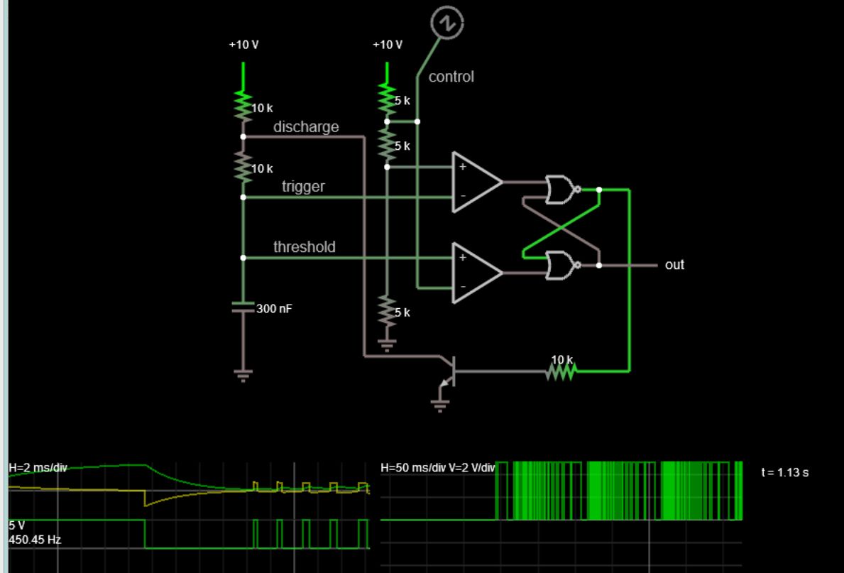
Here is a 10 minute internal design of a 555 timer with a 10Hz sawtooth sweep on Vc
7961623900_1443816360.jpg
for a FM or VCO sweep generator.
 
Status
Not open for further replies.

Part and Inventory Search

Welcome to EDABoard.com

Sponsor

Back
Top