Continue to Site

Welcome to EDAboard.com

Welcome to our site! EDAboard.com is an international Electronics Discussion Forum focused on EDA software, circuits, schematics, books, theory, papers, asic, pld, 8051, DSP, Network, RF, Analog Design, PCB, Service Manuals... and a whole lot more! To participate you need to register. Registration is free. Click here to register now.

Calculating Vout/Vin of a circuit

Status
Not open for further replies.

Mohammed Abrar

Junior Member level 1
Joined
Sep 6, 2015
Messages
15
Helped
0
Reputation
0
Reaction score
0
Trophy points
1
Activity points
103
How do I calculate Vout/Vin of this arrangement:

help.png

I have to do this using the small signal model, I am a beginner level electronics student so a complete explanation would be nice.
 

Simplest and most straight forward explanation would be to replace the MOSFET with it's small-signal model (Pi-Model Preferably). If you just want DC gain then treat all caps (Cgs, Cgd, Csb, Cdb) as open circuits. Now you would sum currents at nodes until you have enough equations with enough unknowns to solve for what you want.

Also I will assume you will neglect back-gate transconductace and Vsb = 0V.
 

I did replace the mosfet with the small signal model but I can't solve it for Vout/Vin.
 

How do I calculate Vout/Vin of this arrangement:

View attachment 121875

I have to do this using the small signal model, I am a beginner level electronics student so a complete explanation would be nice.

Replace the MOSFET with its small signal model. So you have a current source from drain to source, whose value depends on the transconductance as well as the gate-to-source voltage. You don't have body effect in this case, right? Then, consider the output resistance due to channel length modulation. Once you put these together, you basically have one node where you can use KCL - you've reduced the circuit to a very simple linear circuit.

Also consider what happens to VDD in the SSM - AC ground.

Show us what you have and where you're stuck.

ad-page-001.jpg

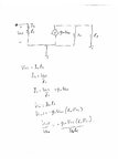
I still have an unknown Ig.
 

1) What is the Rs and why do you have it there?
2) What do we know about Ig of MOSFETs at DC? (Zero)
 

1) What is the Rs and why do you have it there?
2) What do we know about Ig of MOSFETs at DC? (Zero)

Rs is actually Rg.
If Ig is zero then Vout/vin = infinity. Doesn't make sense.
 

Solve for Vout in terms of Vin by doing KCL at drain. That'll give you your required ratio.

In your SSM, you have Ig going through Rs - Ig is current into gate, not into Rs.
 

Solve for Vout in terms of Vin by doing KCL at drain. That'll give you your required ratio.

In your SSM, you have Ig going through Rs - Ig is current into gate, not into Rs.

answer-page-001.jpg

Is this right? Man, I **** at this
 

Status
Not open for further replies.

Part and Inventory Search

Welcome to EDABoard.com

Sponsor

Back
Top