Continue to Site

Welcome to EDAboard.com

Welcome to our site! EDAboard.com is an international Electronics Discussion Forum focused on EDA software, circuits, schematics, books, theory, papers, asic, pld, 8051, DSP, Network, RF, Analog Design, PCB, Service Manuals... and a whole lot more! To participate you need to register. Registration is free. Click here to register now.

Determining maximum operating frequency of a D Flip flop as a phase frequency detecto

Status
Not open for further replies.

amsdesign

Member level 3
Joined
Aug 26, 2015
Messages
67
Helped
0
Reputation
0
Reaction score
0
Trophy points
6
Activity points
550
I am designing a phase frequency detector for a PLL using the standard configuration as shown below.
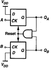
pfd.png

Each D FF is implemented as shown below:
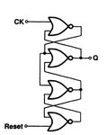
Razavi_DFF.JPG
Can you tell me how I can determine the maximum operating frequency of each Flip flop?
Also, how do the sizing of the CMOS pairs in each gate affect the frequency?
 

Hi,
I think you just apply 2 pulse signals to A,B. After, you change frequency and look at response Qa, Qb. You will compare results with theory. Actually, maximum frequency is relativity.:drevil:
 

Initially I would be tempted to define the maximum operating frequency by the critical path, as being the propagation time of each one of the three NOR gates, added to the propagation time of the AND gate.

However, as there is a symmetry in the circuit, in theory one side should balance the delay of the other, but I believe that the maximum frequency is effectively determined by the asymmetry due to the real world different characteristics of each component, just a guess.
 

The building blocks of the PFD circuit are not exactly D-FFs (the circuit won't work correctly with standard DFFs, by the way).

I presume, you can see the operation frequency liniting effect in a simulation with gate delays. At first sight, it's the minimal input low period required to reset the "bottom" latch, could be something like two or three gate delays.
 

The building blocks of the PFD circuit are not exactly D-FFs (the circuit won't work correctly with standard DFFs, by the way).

Can you explain what you mean by standard DFFs? I simulated the above circuit with each D FF as shown (a cascade of NOR gates) ?


I had two methods in mind to find the max. operating frequency of the FF:

1) For the maximum frequency of the PFD, is it the max. frequency for each FF (using setup, hold time and the critical path timing) ?

2) I plotted the output of the PFD for a constant phase difference (25% of period) for increasing frequencies. At 125 Mhz the PFD did not output the correct phase difference. Is this the right method?


Thank you
 

DFF setup- and hold-time are a timing relation of D and CLK input. They can't be determined for a circuit without a D input. In so far "method 1" isn't applicable.

Method 2 sounds O.K., you should check if the result also depends on phase difference. If my guess in post #4 is correct, it won't.
 

DFF setup- and hold-time are a timing relation of D and CLK input. They can't be determined for a circuit without a D input. In so far "method 1" isn't applicable.

Method 2 sounds O.K., you should check if the result also depends on phase difference. If my guess in post #4 is correct, it won't.


I set a constant phase difference and then increased the frequency. At one point the PFD did not give me the correct phase difference. So it doesn't depend on the the phase difference right?


Also, kindly explain what you meant by this statement in your post #4

The building blocks of the PFD circuit are not exactly D-FFs (the circuit won't work correctly with standard DFFs, by the way).
 

I set a constant phase difference and then increased the frequency. At one point the PFD did not give me the correct phase difference. So it doesn't depend on the the phase difference right?
If you get the same result for other constant phase differences, yes.

- - - Updated - - -

Also, kindly explain what you meant by this statement in your post #4
I reconsidered the point and think now, I was wrong. Should agree with Razavi's statement in RF Microelectronics:
The DFF in Fig. 8.16 may employ different topologies in bipolar and CMOS implementations. In bipolar technology, a standard master-slave configuration with an additional reset input can be used. In CMOS technology, a simple circuit such that in Fig 8.18 proves adequate. Note that the D input is "hidden" here.

Quoted Fig 8.16 and 8.18 are the circuits according to post #1.
 

Status
Not open for further replies.

Part and Inventory Search

Welcome to EDABoard.com

Sponsor

Back
Top