Continue to Site

Welcome to EDAboard.com

Welcome to our site! EDAboard.com is an international Electronics Discussion Forum focused on EDA software, circuits, schematics, books, theory, papers, asic, pld, 8051, DSP, Network, RF, Analog Design, PCB, Service Manuals... and a whole lot more! To participate you need to register. Registration is free. Click here to register now.

[SOLVED] Ground Splitting Issue of Mixed-Signal Layout

Status
Not open for further replies.

abonic

Junior Member level 2
Joined
Dec 5, 2012
Messages
23
Helped
0
Reputation
0
Reaction score
0
Trophy points
1,281
Activity points
1,431
Dear all,
I'm doing the layout for a mixed-signal system on the P-SUB CMOS Process these days, there're two grounds AVSS & DVSS for Analog domain and Digital Domian.
Both Analog Core and Digital Core are enclosured by two dedicated Nwell Guarding Rings separetely, thus the Calibre LVS for both Analog Core & Digital Core pass with no error and no P-SUB warning.
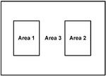
Ground Issue.png
However, when they are connected at the top level, there're 3 Areas on the P-SUB. Suppose, Area 1 is for AVSS, Area 2 is for DVSS, where should the rest part of the P-SUB (Area 3, actually enclosured by the Nwell strip of the PAD Ring) be connected so as to achieve a good noise-immunity performance.
I suppose it is a common issue in the mixed-signal layout design, which has a sophisiticated solution, could anybody help

Thank you!
 

... they are connected at the top level, there're 3 Areas on the P-SUB. Suppose, Area 1 is for AVSS, Area 2 is for DVSS, where should the rest part of the P-SUB (Area 3, actually enclosured by the Nwell strip of the PAD Ring) be connected so as to achieve a good noise-immunity performance.

Via separate p+ guard rings around each Area 1 and Area 2, both connected via contacts and metal 1 to the common VSS (GND) point at top level.
 

Via separate p+ guard rings around each Area 1 and Area 2, both connected via contacts and metal 1 to the common VSS (GND) point at top level.
Dear erikl,
According to you suggestion, AVSS & DVSS are finally shorted at the top level. However, it is not what I expected.
AVSS & DVSS are typically separated at the PAD Ring, thus the PAD Ring is typically divided into several sections (i.e. through cellcut), each has individual Power Supplys for Core and ESD.

I'm quite confusing that if I use a PAD Ring with separate sections in order to separate AVSS & DVSS, they are still shorted through the common P-SUB.

Therefore it seems not so easy to completely separate AVSS & DVSS, is that the case?
 

According to you suggestion, AVSS & DVSS are finally shorted at the top level. However, it is not what I expected.
That's what you told in your original post:
... However, when they are connected at the top level, there're 3 Areas on the P-SUB. ...


AVSS & DVSS are typically separated at the PAD Ring, thus the PAD Ring is typically divided into several sections (i.e. through cellcut), each has individual Power Supplys for Core and ESD.

I'm quite confusing that if I use a PAD Ring with separate sections in order to separate AVSS & DVSS, they are still shorted through the common P-SUB.

Therefore it seems not so easy to completely separate AVSS & DVSS, is that the case?

Not completely, but it is possible to junction-isolate psub areas by (deep) n-wells, which possibly reach down to a buried n+ layer as to completely isolate single psub areas by a blocked junction.

Even if this is not the case, the single psub areas are contacted by many low-ohmic p+ diffusion taps (preferably a p+ tap ring), additionally protected by an n+ guard ring against straying charge carriers. So the low-ohmic p+ taps - connected by contacts to metal1 - all have a low-ohmic connection to the common top level connection point (VSS = GND) or to their still separated pads.

Sure there's still a connection of all these separated psub areas via their common p substrate, but this is a relatively high-ohmic connection compared to the individual p+ taps connections, which all lead their VSS currents via a highly doped p+ region and metal to their common connection point, respectively to their still isolated pads.
 
  • Like
Reactions: abonic

    abonic

    Points: 2
    Helpful Answer Positive Rating
Dear erikl,
You've explained this issue throughly and quite comprehensible.

Thanks a lot!
 

Status
Not open for further replies.

Part and Inventory Search

Welcome to EDABoard.com

Sponsor

Back
Top