jasensio
Junior Member level 1
Hi everyone!
My design works up to 4 GHz.
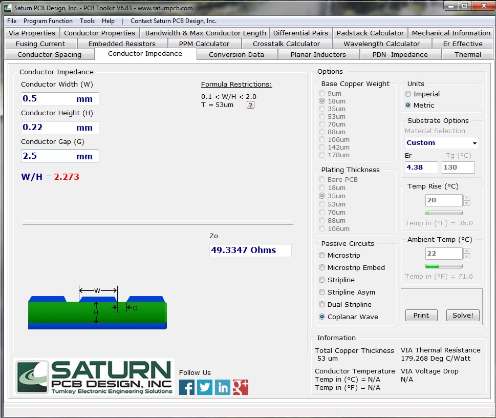
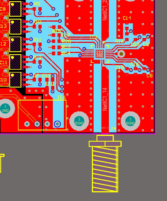
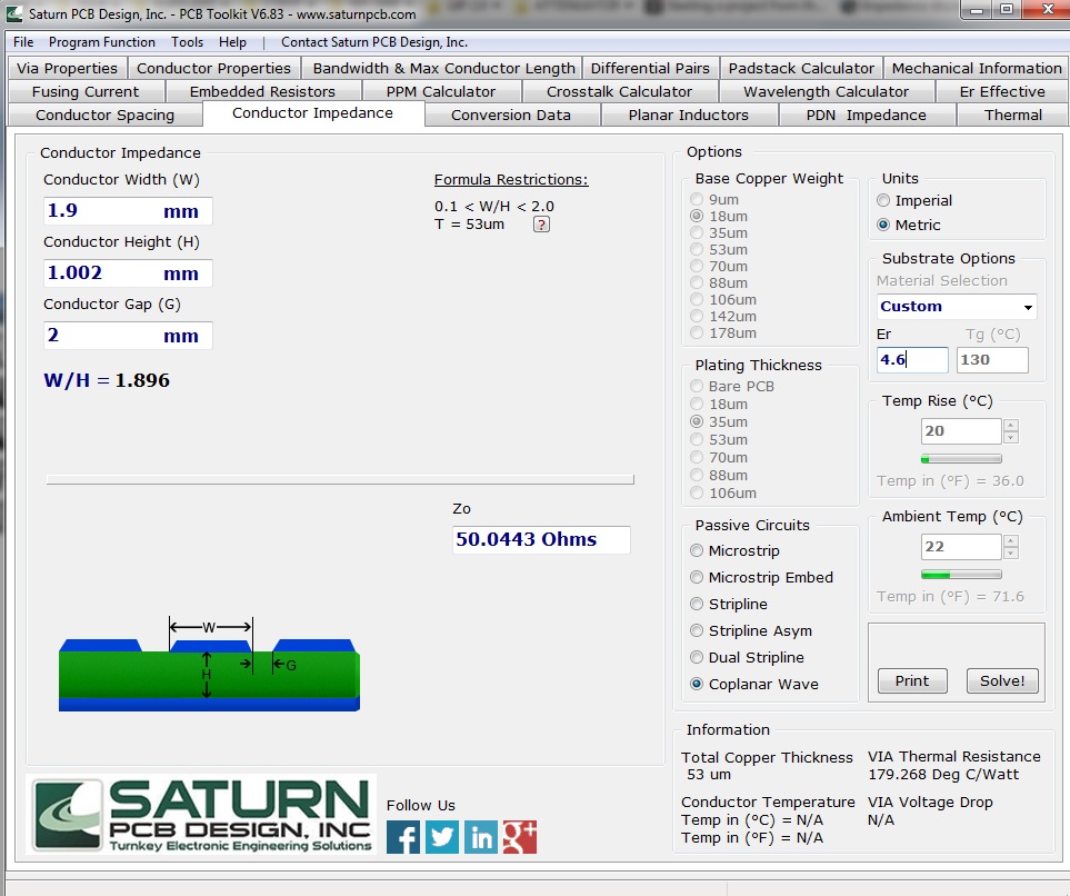
As shown in the attached pic, I have an SMA connector soldered to the board.

The track width is 0.5 mm as the connector pin diameter is 1 mm roughly.
There will be impedance discontinuity due to this difference between the track width and the connector?
Thanks,
Jose
My design works up to 4 GHz.
As shown in the attached pic, I have an SMA connector soldered to the board.
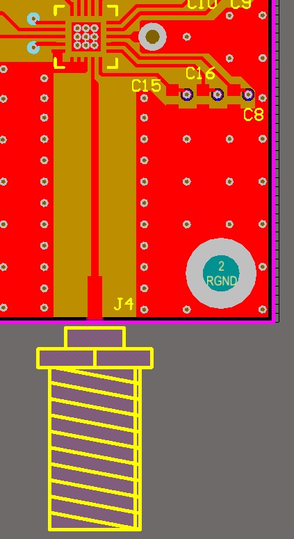
The track width is 0.5 mm as the connector pin diameter is 1 mm roughly.
There will be impedance discontinuity due to this difference between the track width and the connector?
Thanks,
Jose