Continue to Site

Welcome to EDAboard.com

Welcome to our site! EDAboard.com is an international Electronics Discussion Forum focused on EDA software, circuits, schematics, books, theory, papers, asic, pld, 8051, DSP, Network, RF, Analog Design, PCB, Service Manuals... and a whole lot more! To participate you need to register. Registration is free. Click here to register now.

[Moved]: Continuous Time Sigma Delta ADC Integrators

Status
Not open for further replies.

Shady Ahmed

Member level 5
Joined
Jan 26, 2013
Messages
86
Helped
2
Reputation
4
Reaction score
2
Trophy points
1,288
Activity points
2,042
I am designing a 3rd order sigma delta ADC with OSR = 32 , Fsampling = 64 MHz, with 1.5 bit comparator. The design is in 0.13um technology.

The target peak SNR from the system design (i used Schreier toolbox) was 76 dB.
After generating the system coefficients, i verified it on Cadence using ideal components.

The system peak SNR was 76 dB using Ideal op-amps (for the RC integrators), ideal feedback DAC & NON IDEAL (CMOS) comparator.

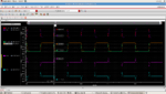
The system schematic showing the series of RC integrators, the feedback DAC & The comparator.

Picture1.png

Now , i started designing the CMOS op amps, i have gone through several op amps trials however the system SNR degradation is HUGE, the best result i reached was 37 dB (instead of 76 dB for the ideal op amps)


1st op amp design trial:

Schematic (i used a VCVS as the correction op amp in the CMFB , i'll replace it later if the op amp works)
The current in the second stage = 85 uA.
op amp trial 1.1.png

The op amp Bode Plots, since the sampling frequency = 64 MHz, the designed op amp GBW ~ 3 fs = 200 MHz, with Phase margin = 61 & DC gain = 46.7 dB

op amp trial 1.2.png

The CM bode plots & stability summary (generated using the stb analysis from the probe shown in the schematic)

op amp trial 1.3.png

Finally , the PSD of the Sigma Delta ADC achieving ONLY 37 dB!!

op amp trial 1.4.png

I had a few other op amp trials with different GBW & DC gains, but i had no luck, 37 dB is the best result i got.

GBW , GAIN & Phase margin are the only design parameters i was thinking of while designing the op amp, am i missing something else? are there any other considerations i should take in the design?


Help me please and thanks for your time.
 
Last edited:

Re: Continuous Time Sigma Delta ADC Integrators

I'd say check input output ranges but it looks like they're under correct bias in DC. Still I'd suggest checking if the transient signal exceeds their range.

Also, do you see any ringing, or very fast spikes? Especially at cmfb node. If this is the case, maybe you're not simulating the opamp with the correct loading that it is subjected to in the ADC. Also for better modelling add poles to your CMFB, this may also cause troubles because of huge currents flowing from Cgd capacitor when the vcvs responds very fast.
 

Re: Continuous Time Sigma Delta ADC Integrators

I'd say check input output ranges but it looks like they're under correct bias in DC. Still I'd suggest checking if the transient signal exceeds their range.

The output ranges of the integrators in the transient simulation of the ADC are manageable and can be tolerated by the op amps swings.

Also, do you see any ringing, or very fast spikes? Especially at cmfb node.

I designed several op amps with Phase margin ranging from 45 to 65 degree so on its own, there is no ringing or fast spikes at the output (I'll still check at the CMFB point).

If this is the case, maybe you're not simulating the opamp with the correct loading that it is subjected to in the ADC. Also for better modelling add poles to your CMFB, this may also cause troubles because of huge currents flowing from Cgd capacitor when the vcvs responds very fast.

I am really interested in this point, how do i decide the capacitive load i should design the op amp for ? I mean if , for instance I'll be using C= 1pF in the feedback path of the RC integrator , who do i know what value of capacitive load to design upon in the op amp ???

Thanks for your time.
 

Re: Continuous Time Sigma Delta ADC Integrators

I went back to the op amp and performed a step response with a unity gain amplifier setup.
shown in the next figure the test bench schematic:
step response test bench schematic.png

shown in the next one, the DM stb analysis of the diff probe appearing in the schematic
DM stb  analysis.png

And the transient output is shown here (input step pulse has the same frequency of the ADC clock)
transient step pulse response.png


It seems that the performance isn't quite good & even the output CM value changes.. what should i do?
plus , is the step response test sufficient or should i perform the test with the integrator setup with exactly the same RC values used in the ADC?

- - - Updated - - -

Also, here are the results of testing the op amp as an integrator with an input sine wave (with frequency 10 MHz) , RC are selected such that :
omega *R * C = 1

Sin wave integrator test.png


sine wave stb summary.png
 

Attachments

  • Step response test.png
    Step response test.png
    96.9 KB · Views: 132

Re: Continuous Time Sigma Delta ADC Integrators

For the output loading: It should be feedback cap + the next stages loading effect. However for this to be accurate your virtual ground has to stay still.

For the transient step: The transient step you apply is not a huge step but your opamp fails to catch up. So it may not be slewing but it may be just that your bandwidth is small. What accuracy do you need is another question you need to answer.

For simulations in general: Yes you should simulate each sub block individually to come up with specifications for them. But there's something I don't understand, you showed that your opamp wasn't fast enough in the first sim but in the second sim you're showing it's giving nice and clean response, how come?

Also since this is continuous time all those errors occurring at transitions are going to affect your final results. So your opamp specifications should be even more strict. When you say that you verified with ideal elements, did you mean ideal elements + band limit or just vcvs everywhere? Because you should definitely find what are good specs for your opamps.
 
Re: Continuous Time Sigma Delta ADC Integrators

For the transient step: The transient step you apply is not a huge step but your opamp fails to catch up. So it may not be slewing but it may be just that your bandwidth is small. What accuracy do you need is another question you need to answer.

The op amp Gain Bandwidth is supposed to be 200 MHz , so i think it should have been able to catch up with the step response with 64MHz frequency, maybe 60 degree phase margin is little too much ? or maybe it is the slew rate?

But there's something I don't understand, you showed that your opamp wasn't fast enough in the first sim but in the second sim you're showing it's giving nice and clean response, how come?

Please keep in mind the different setup , 1st test was a step response test with a unity gain amplifier with input frequency = 64 MHz.
While the 2nd test was an integrator with sine wave input with frequency 10 MHz.

Also since this is continuous time all those errors occurring at transitions are going to affect your final results. So your opamp specifications should be even more strict.
If you mean the spikes in the CM node, where do u think it come from ? CM loop stability ?

When you say that you verified with ideal elements, did you mean ideal elements + band limit or just vcvs everywhere? Because you should definitely find what are good specs for your opamps.

I mean the ADC composed of : full ideal op amp (using ONLY vcvs) , Ideal DAC (using ideal switches) & CMOS comparator.
What do u suggest to better implement the ideal op amp? what else should i use other than the vcvs?

Thanks again, i appreciate it.
 

Re: Continuous Time Sigma Delta ADC Integrators

1- With 64 MHz frequency it looks about right, I guess. I didn't know your operating parameters and didn't bother to look at time axis, my bad. So your opamp is not really good at doing its thing with 64 MHz square wave.

2- What I meant was the last results where you show a nice and clean response to square wave. Then I realized this was a slowed down version, I should've checked before, my bad again. Also looking at transient waveforms of sine waves is not a good way of characterizing an integrator. It just shows you that it's working, says not much about its performance.

3- What I mean is this is not a sampled system, any errors happening there are going to get integrated. So it's normal to expect more strict specs when designing a continuous time DSM.

4- I think this is the real part you should focus on. When designing you do all those models to go from concept to design parameters. But "a working opamp" is not a design parameter. You need to extract BW required for your opamp, offset and a lot of stuff from your model that runs lightning fast so that you can make sure everything is working and then move on to transistor level which takes seriously longer.

Leave everything else ideal, but instead of just vcvs put vcvs + RC + a buffer vcvs as your opamps. And see if a perfect opamp with limited bandwidth is doing the thing in your design. If so what kind of bandwidth is required for your target SNR? Then if you want you can add slewing and other stuff to your model, I'd advise using verilogA, it's easy and does acceptable in these kind of stuff.

So my point is, I don't see anything fundamentally wrong in your opamp, but I also can't see if you're trying something impossible or not. And neither do you, so you should check. I'm sure there would be people who can easily tell if these specs suit your needs but I think you should go through this experience so that in the future it'd be easier. Sorry if I mislead you but that's all I can think of.
 
OP, did you figure out why ?
I feel like according to you PSD, you should have more fft points.
 

Status
Not open for further replies.

Similar threads

Part and Inventory Search

Welcome to EDABoard.com

Sponsor

Back
Top