Souljah44
Junior Member level 1
Hello,
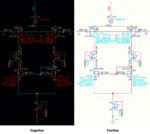
Please refer to the images attached.
I'm hoping someone can shed some light on this because I'm really confused about this. I have a simple diff pair where I sweep, one input (ip) and hold the other (in) at vdd/2. At ip = 0V, I would expect the entire bias current to flow through the device connected to "ip" and when ip is at VDD, I would expect the entire current to flow through the device connected to "in". The red waveform is the current through "ip" and the green is the current through "in" device. The yellow trace is just the sweep voltage on "ip".
The y-axis on the left is current and the one on the right is voltage.
When ip=0V, the waveforms make sense but not when "ip" approaches vdd. The current levels don't get near where they should be. If I remove the nmos devices, the waveforms match the theory. I've swept both width and length of the nmos devices to no avail.
Can anyone explain to me what might be going on? Am I missing something here?
Thanks