Continue to Site

Welcome to EDAboard.com

Welcome to our site! EDAboard.com is an international Electronics Discussion Forum focused on EDA software, circuits, schematics, books, theory, papers, asic, pld, 8051, DSP, Network, RF, Analog Design, PCB, Service Manuals... and a whole lot more! To participate you need to register. Registration is free. Click here to register now.

Lower Vth after QRC extraction

Status
Not open for further replies.

cira529

Newbie
Joined
Oct 12, 2013
Messages
3
Helped
0
Reputation
0
Reaction score
0
Trophy points
1,281
Activity points
1,300
Hi everyone,

I am new on this forum and relatively new on analog design.
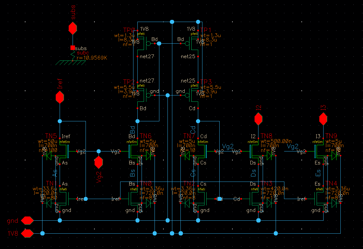
I finished layout design of my low-voltage current mirror (100:1). I used 2D common centroid for better matching. After extraction spectre gave me Vth=335mV (346mV in schematic) for my unity MOSFET TN3. Everything else is same.

What is mechanism behind this lowering?
Thank you.
 

The only thing which is going to my head is a proximity effect bounded with substrate contact distance to diffusion of this nfet, but I'm not sure if this effect is modeled in your IBM process. You have to check documentation for it.
 

Thank you Dominik,

I use 180nm process and WPE is not a problem.
As u can see I have ratio 10:1 between TN1 and TN0 but 8:1 between TN2 and TN3.
When I was doing spectre simulations I had 10:1 current mirroring for 8:1 MOSFET ration, Vth(TN2)=335mV and Vth(TN3)=346mV.
Also I have 80 fingers for TN1, 8 fingers for each of TN0 and TN2 and when extracted every finger have 335mV like in schematic even the main one (TN3) who had 346mV.
I am confused. What do you think?
 

Status
Not open for further replies.

Part and Inventory Search

Welcome to EDABoard.com

Sponsor

Back
Top