Continue to Site

Welcome to EDAboard.com

Welcome to our site! EDAboard.com is an international Electronics Discussion Forum focused on EDA software, circuits, schematics, books, theory, papers, asic, pld, 8051, DSP, Network, RF, Analog Design, PCB, Service Manuals... and a whole lot more! To participate you need to register. Registration is free. Click here to register now.

Flyback primary waveform ramps up, spikes on secondary

Status
Not open for further replies.

bowman1710

Full Member level 3
Joined
Nov 8, 2014
Messages
183
Helped
6
Reputation
12
Reaction score
6
Trophy points
18
Activity points
1,604
Hi guys,

I have a flyback design taking 50V to 12V @ 1.25A, switching at 1MHz. The transformer has a LP of 66uH with 36T primary and 9T secondary (3.5 ratio). The switching waveform attached is the primary waveform. The primary ramps to over 100V, on the secondary side the the waveforms have large spikes. Any ideas where i have gone wrong with my transformer?
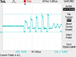

waveform.png
 

Are you sure that the flyback converter is regulated for secondary voltage of 12V? The waveform rather looks like 24V secondary voltage with the given turns ratio.
 

Yes I am getting 12V out, just ive never come across this ramping input waveform and spikes on the secondary

this is the equation i used to calculate the ratio

formula.PNG
 
Last edited:

The primary ramps to over 100V

Since that is greater than your supply V, it sounds as though your primary has no snubber network.

It is common for a snubber to be installed across the primary. The reason it is needed, is that when you switch off supply current, a strong voltage spike is generated by the transformer. (A characteristic of inductors.) Ringing may also be generated.

There are various snubber configurations. Adding one on your primary may or may not solve the large spikes at your secondary.
 

Also I'm wondering what causes the voltage to plateau at ~35V for a little while before the characteristic ringing shows up.
 

It looks like the secondary is not connected for 3 micro secs, then the circuit settles down. Or it could be that there is a short circuit on the secondary for this time period and the spikes are due to primary leakage inductance. Could it be that the transformer core is being pushed into saturation by the charging current of the reservoir capacitor?
Frank
 

Thanks for you help guys, i had a feeling that it might have something to do with either the snubber circuit, transfomer or both, it does have a snubber on it but i think that it must not be clamping the voltage down enough possibly. I am going to get a pre-made transformer from digikey that suits the bill and go from there. I wonder if my inductance primary inductance may be wrong with a switching frequency of 1MHz???? I will keep the post updated to let you know how I get on with it.
 

I will keep the post updated to let you know how I get on with it.
Obviously, the first and urgently needed "update" would be a complete schematic...
 
schematic.PNG

sorry yes you are right, it is this, but i have changed the transformer for it to give a 12V output at 15W, with what was mentioned in post #1
 

Circuit looks regular. I keep my point that the waveforms don't fit the claimed transformer ratio and voltages.
 

Hi,

check if D1 = UPS840 works like desired.
It should be high ohmic in one direction and low ohmic in the other direction.
Also check if it is mounted in correct direction.

if this is OK, then check if Co1, Co2, and Co3 are high frequency, low esr capacitors. Standard electrolytic don´t work here.
In either case I recommend to add a ceramics capacitor with short and wide wiring to transformer/diode. Use at least 10uF and 50V.

Klaus
 

I keep my point that the waveforms don't fit the claimed transformer ratio and voltages.

Why doesn't the primary waveform i posted illustrate the 3.5:1 ratio I stated in post #1?

Also check if it is mounted in correct direction.

if this is OK, then check if Co1, Co2, and Co3 are high frequency, low esr capacitors. Standard electrolytic don´t work here.
In either case I recommend to add a ceramics capacitor with short and wide wiring to transformer/diode. Use at least 10uF and 50V.

The board was working fine when i had it standard with the 3.3V @ 3A, the caps are ceramics and the diode is fine. It wasnt until i changed the transformer on the board to output 12V until i had this issue. Hence why ive assumed its something ive done with the transformer rather then anything else. I agree with what bradtherad said:

It is common for a snubber to be installed across the primary. The reason it is needed, is that when you switch off supply current, a strong voltage spike is generated by the transformer. (A characteristic of inductors.) Ringing may also be generated.

It is likely i haven't allocated for the need for the change in the snubber circuit but think there is also wrong with the trasformer, whether it be primary inductance, leakage inductance turns ratio etc?
 

Hi,

is the wiring direction of all windings correct.
I mean: during Q2 is closed:
* transformer pin4 is positive with respect to pin3
* transformer pin1 is positive with respect to pin2
* transformer pin7/8 is positive with respect to pin5/6

when Q2 is open the voltage direction changes.

Klaus
 

Why doesn't the primary waveform i posted illustrate the 3.5:1 ratio I stated in post #1?
Ideally the primary flyback voltage should be (Vout+0.5)*N+Vin, which is about 94V. You're showing about 150V. Which happens to be the exact VDD rating of your FET...

And I still can't think of a good explanation for the primary voltage plateauing at ~35V, can you show a secondary waveform as well? Preferably under steady state and at startup?

The board was working fine when i had it standard with the 3.3V @ 3A, the caps are ceramics and the diode is fine.
The schematic says the output caps are rated for 6.3V, you should change them to be 16V or more.
It wasnt until i changed the transformer on the board to output 12V until i had this issue. Hence why ive assumed its something ive done with the transformer rather then anything else.
Changing the transformer alone won't change the output voltage. Did you adjust the feedback resistors (R13 and R14) to change the setpoint? Is the auxiliary winding still okay with the different transformer?
 

Hi Guys update on the previous, I tried a new transformer which still gave me the same issue. I then tried changing the opto driver and opto with a FOD2742 and all works fine now, can't see why the LT4430 was causing me issues but for some reason it was. I checked all the values i needed for compensation and they seem fine, nothing that would of given me that sort out output and primary any way, but i'm sticking with what I know and keeping the FOD, glad i got it working for my own sanity really.
 

I'm looking at the values for your snubber circuit (post #10). You may see undesired high volt levels at pin 3 of T1, due to using a small value for C8, and large value for R3.

I believe C8 should be increased several times, and R3 decreased to 1k in order to discharge C8 sufficiently.

R3 is then required to dissipate 2 to 4 W as heat.

Do not reduce R3 below a few hundred ohms. The lower it is, the more power you waste.
 

Status
Not open for further replies.

Similar threads

Part and Inventory Search

Welcome to EDABoard.com

Sponsor

Back
Top