Continue to Site

Welcome to EDAboard.com

Welcome to our site! EDAboard.com is an international Electronics Discussion Forum focused on EDA software, circuits, schematics, books, theory, papers, asic, pld, 8051, DSP, Network, RF, Analog Design, PCB, Service Manuals... and a whole lot more! To participate you need to register. Registration is free. Click here to register now.

Sigma Delta ADC Integrators

Status
Not open for further replies.

Shady Ahmed

Member level 5
Joined
Jan 26, 2013
Messages
86
Helped
2
Reputation
4
Reaction score
2
Trophy points
1,288
Activity points
2,042
Hi,
I am designing a 3rd order, 1.5 bit (= 3 Level) quantizer Continuous Time Sigma Delta ADC, with maximum input frequency 1 MHz, OSR = 32.

The target SQNR = 75 dB.
The system achieves the desired SQNR using CMOS comparator, ideal op-amp & Ideal DAC.

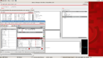
when i tried to design the CMOS op-amp, i achieved the following specs:
GBW: 200MHz
Open Loop DC Gain= 40 dB
Phase Margin= 43 degree.

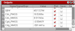
However, when i simulated the system with that op-amp , the performance is HUGELY affected, the achieved SNR = 32 dB !!!!!

What did i do wrong? are there any specs that i forgot about and should take care of in the op-amp)?
 

You should be able to see in a simulation which real OP parameters have the greatest impact. I guess, low gain will be a problem.
 

You should be able to see in a simulation which real OP parameters have the greatest impact.


I simulated the ADC and plotted the output of the comparator (D1 , D0, D_1) , and the integrator outputs.
I can't quite get where the problem come from

post ^% figure 2.pngPost ^% figure 3.pngPost ^% figure 4.pngpost ^% new figure 1.pngpost^% ALL outputs.pngPost^% figure 2.png


Here are a few plots of the output with different zoom.
The first note is that the integrators are not saturated.
However, i doubt that those VERY FAST changing ripples are the cause , is that some sort of instability ? maybe CMFB loop instability or bad Phase Margin?

I guess, low gain will be a problem.

Could that be possible? is a gain of 40 dB each integrator not sufficient for a 3rd order ADC with 75 target dB ?!!
 

I think this maybe due to the CMFB circuit,, and since i'll have to implement real CMFB circuits anyway, i started looking into CMFB circuits architectures.
Any specific architectures for 2 stage op-amps? or should i replace the vcvs with an equivalent op-amp?
 

A simple differential one-stage amp with constant current source and diode connection load should do. No stability problem.
 

A simple differential one-stage amp with constant current source and diode connection load should do. No stability problem.
Do u mean replacing the op-amp (the error amplifier) with the differential one stage amp??
Because i read about some CMFB architectures (check the images for examples)
CMFB.PNG

and i wasn't sure whether to just implement the op-amp or follow one like this
 

Do u mean replacing the op-amp (the error amplifier) with the differential one stage amp??
Because i read about some CMFB architectures (check the images for examples)
View attachment 118988

This is a good example for a differential one-stage opAmp. You could even save one differential pair (M23, 24, 27), if you merge the 2 outputs from the opAmp (e.g. via 2 RC combinations) to the M21 input.
 
any help ? The op amp with the ideal vcvs in the CMFB circuit still affects the Sigma Delta ADC performance greatly!! I just want to make sure it works before consuming time designing the real CMFB circuit.
 

The op amp with the ideal vcvs in the CMFB circuit still affects the Sigma Delta ADC performance greatly!!

Could you show how you connected the vcvs-CMFB to your opAmp?
 

I'm not sure if your CMFB circuit works in the right direction: Your diffstbprobes look like (non-inverting) buffers, but - if they work like iprobes - they might have a large output impedance, so creating gain loss in connection with the resistors -- check this.

Then you connect the common output of the resistors to the negative vcvs input, which means an inversion. Hence rising outputs create falling v_cmfb, which again causes rising outputs: positive feedback, so the opAmp would leave its good operation point.

Because I don't know exactly the working effect of the diffstbprobes, I'm not sure about this, but I think it's worth to be checked.
 

I'm not sure if your CMFB circuit works in the right direction


I understand that theoretically, the loop has positive gain, however, when i was designing the op-amp, i spent a lot of time connecting the inputs to the vcvs the other way, and it didn't work at all, the outputs would always saturate to VDD , however , the connection as shown in the image, got the op amp to work (on its own , in a test bench)

Plus, when i connect the output of the resistors to the positive vcvs input, the ADC doesn't work at all (after few cycles, the output of the integrators saturate) which means that this connection is a positive feedback, unlike connecting them to the negative, which just degrades the performance greatly, but at least it works.

I know that doesn't seem to make sense, but i thought maybe vcvs works in a way that i don't understand.

Your diffstbprobes look like (non-inverting) buffers, but - if they work like iprobes - they might have a large output impedance

I read somewhere that the diffstbprobes act as short circuits in DC/trans analysis , so i don't think it's causing any problems, and i also tried to remove them which didn't make any difference in the performance.

Thanks for your time.
 

I'm not sure if your CMFB circuit works in the right direction

I was wrong with this remark, sorry: up to the vo_2 outputs there's another inversion (3 in total), hence negative feedback, indeed.

Are you sure that the CMFB part of the opAmp is the culprit for the SNR degradation? Did you try with a LF low pass filter (e.g. a cap from the resistors' common connection point to GND), if this cures the degradation?
 

Are you sure that the CMFB part of the opAmp is the culprit for the SNR degradation?

No, i am not sure that the CMFB part is the culprit.

Did you try with a LF low pass filter (e.g. a cap from the resistors' common connection point to GND), if this cures the degradation?

Do u mean to compensate the CMFB detector? (i.e : add capacitors in parallel with the R_CMFB?)


Ok, i think at this point it'd be better if i provide the whole op-amp plots

1- The op amp schematic with the DC Node voltages and DC op points displayed
Op-Amp schematic.png


2- The DM bode plots
DM Bode plots.png

3- The CM bode Plots

CM Bode Plots.png


N.B: the system's clock frequency = 64 MHz,
so i chose the op amp GBW to be around 180 MHz as shown, with PM = 41 degree (with Cload = 1 pF, which i chose to be the value of the feedback capacitor in the integrator)

The common mode stability analysis :
GBW = 416 MHz, PM = 29 degree.

Thanks for your time , i appreciate it.
 

Did you try with a LF low pass filter (e.g. a cap from the resistors' common connection point to GND), if this cures the degradation?

Do u mean to compensate the CMFB detector? (i.e : add capacitors in parallel with the R_CMFB?)

No, that would be a high pass filter, i.e. it would favour high frequencies. I'd suggest the contrary: s. the underlined words above, in order to suppress possible noise or oscillations from the CMFB, to find out if the degradation is a result of the CMFB.

I think you could also generate the Bode plots of your opAmp without using the CMFB, supplying the ref voltage instead of v_cmfb.


Ok, i think at this point it'd be better if i provide the whole op-amp plots
Your Bode plots look quite well; I can't find any hint for so much SNR degradation.
 

I think you could also generate the Bode plots of your opAmp without using the CMFB, supplying the ref voltage instead of v_cmfb.

Here are the modified schematic along with the new bode plots, it looks the same.
no cmfb schematic.png

no cmfb bode plot.png
 

Here are the modified schematic along with the new bode plots, it looks the same.

So it's clear: not the CMFB part is the culprit, but the opAmp itself (in comparison to an ideal opAmp). Or did you perhaps change anything else, additionally?

It's quite normal that you loose SNR due to substitution of ideal cells by real ones, but it shouldn't be so much (> 40dB in your case).

Anyway, for a 1.5bit quantizer, the integrator shouldn't be such sensitive!? What's the value of the feedback capacitors, in comparison to the inherent MOSFET caps (which do not exist for ideal cells)?
 

So it's clear: not the CMFB part is the culprit, but the opAmp itself (in comparison to an ideal opAmp). Or did you perhaps change anything else, additionally?

No, i didn't change anything else, i just removed the CMFB from the schematic, and simulated with the following schematic shown in the figure (by adding resistors followed by source of 0.6V)
schematic with cmfb forced.png


What's the value of the feedback capacitors, in comparison to the inherent MOSFET caps (which do not exist for ideal cells)?

The feedback capacitor = 1pF while the next figure shows the values of Cds & Cgd of the PMOS & NMOS of the output (second) stage


Thanks for you time.

- - - Updated - - -

(The capacitor values)
Capacitances Values.png
 

Attachments

  • Capacitances.png
    Capacitances.png
    311.9 KB · Views: 63
  • Capacitances Values.png
    Capacitances Values.png
    8.4 KB · Views: 71

The feedback capacitor = 1pF

Seems all to be ok - I don't know what could be wrong. I'd suggest to continue with your full system analysis with the SNR result, and exchange any system elements/devices - one after the other, as FvM suggested in the 2nd post - until you find the culprit.

Perhaps you could show the corresponding test bench?
 

Status
Not open for further replies.

Part and Inventory Search

Welcome to EDABoard.com

Sponsor

Back
Top