Continue to Site

Welcome to EDAboard.com

Welcome to our site! EDAboard.com is an international Electronics Discussion Forum focused on EDA software, circuits, schematics, books, theory, papers, asic, pld, 8051, DSP, Network, RF, Analog Design, PCB, Service Manuals... and a whole lot more! To participate you need to register. Registration is free. Click here to register now.

4 layer stackup differential pair for USB, Impedance question

Status
Not open for further replies.

Jester

Full Member level 6
Joined
Aug 18, 2012
Messages
377
Helped
7
Reputation
14
Reaction score
7
Trophy points
1,298
Location
.
Activity points
4,754
I'm routing a 4 layer board with a USB2.0 differential pair.

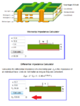
The application note has an example stackup for a 4 layer FR-4 board as shown below (top image). The example includes trace width and spacing for a 90Ω differential pair.

When I enter these parameters into either of the calculators I have, they both give the same result of about 103Ω, also shown below.

Both calculators I have show the stackup as a 2 layer board, however I would think (perhaps incorrectly) that additional layers below what is shown would have minimal impact on the impedance of the traces above the ground plane, but perhaps this is a faulty assumption?

Can anyone explain the 90Ω vs. 103Ω discrepancy?

If the discrepancy is as a result of the 4 layers stackup vs. the 2 layer stackup shown in the calculator, does anyone have a link to a calculator where I can enter all the required parameters for a board as shown in the top image?
Stackup-Impedance1.png
 

It's unclear how the 4 layer stackup should be related to the impedance calculation because there's no ground plane in the 4-layer stackup. What's your intended transmission line design for the USB?

In most cases, you'll probably decide for a microstrip with a ground plane on the layer below. USB has by the way also a (rather loose) specification for the common mode impedance because it's using single ended signalling.

Sorry, clear in my mind, but not in the information posted. Midlayer 1 will be ground, and Midlayer 2 will be Vcc, top and bottom are signal layers, and the USB signals will be very short ~4mm on the top only (the connector is adjacent to the driver).
 

In this case, only the substrate (prepreg) height between top layer and mid-layer1 has to be considered for the calculation.
 
  • Like
Reactions: Jester

    Jester

    Points: 2
    Helpful Answer Positive Rating
One difference between the two calculators is that the coupled (differential) line calculator does not include metal thickness. When metal thickness is included, line impedance goes down.

It goes down even more if you include solder resist, and that might be the difference between your 90 Ohm from the appnote and the calculated 103 Ohm.

With line length of 4mm all this isn't critical.
 
  • Like
Reactions: Jester

    Jester

    Points: 2
    Helpful Answer Positive Rating
According to my tools, surface coating make the biggest difference for the shown geometry, metal thickness only to a small extent.

In real life, varying substrate height, etching tolerances and loosely defined FR4 Er will have the strongest impact. But fortunately, USB impedance isn't too critical.
 
  • Like
Reactions: Jester

    Jester

    Points: 2
    Helpful Answer Positive Rating
Thanks FvM and Volker
 

Status
Not open for further replies.

Part and Inventory Search

Welcome to EDABoard.com

Sponsor

Back
Top