Continue to Site

Welcome to EDAboard.com

Welcome to our site! EDAboard.com is an international Electronics Discussion Forum focused on EDA software, circuits, schematics, books, theory, papers, asic, pld, 8051, DSP, Network, RF, Analog Design, PCB, Service Manuals... and a whole lot more! To participate you need to register. Registration is free. Click here to register now.

fpga and xcf04 connection

Status
Not open for further replies.

morykeys

Newbie level 5
Joined
Apr 17, 2015
Messages
10
Helped
0
Reputation
0
Reaction score
0
Trophy points
1
Activity points
81
hello
i'm new in fgpa designing and it's the first time i'm working with hardware
my question is :
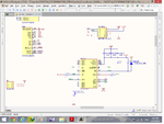
1- is the connection between xcf04 and fpga (xc3s400) right? in other words does it work?
2-if i take tdo from xcf04 and connect tdi to fpga it works or not?

regards
 

Attachments

  • fpga xcf.png
    fpga xcf.png
    126 KB · Views: 112

I doubt that the "DONE" node will achieve a legal logic high level as it's shorted by a red LED.
 

so you're telling me it works properly?
 

you are seeing my circuit are the connection between fpga ,xcf, connetor right or not?
 

Did you read the document (especially page 82)? Compare your schematic and the reference design. You will get your answer.
 

sir yes i did see page 82.
in this mode tdi goes to fpga and tdo is taken from xcf
in mu circuit tdi goes to xcf and tdo is taken from fpga as you see in the picture ?
now all i'm saying does my circuit work because i saw it in xcf datasheet.
 

I doubt that the "DONE" node will achieve a legal logic high level as it's shorted by a red LED.
Yes it is marginal but should work.

660nmD Red LED at 0.4mA will be around 1.6V ( SMD)
640nmD Red LED at 0.3mA will be around 1.7~1.8V (SMD)

assume a 3.3V driver and an LVCMOS25 receiver that has a VIH = 1.7V and the VIL = 0.7V. (actual threshold is in the middle around 1.2V depending on temperature.

Reducing 4.7K to 1K will make it brighter and increase 0.1~0.2V in case of noise for input to next stage of DONE .

But possibly, ok as is, but dim.
 

assume a 3.3V driver and an LVCMOS25 receiver that has a VIH = 1.7V and the VIL = 0.7V. (actual threshold is in the middle around 1.2V depending on temperature.

According to xcf04 datasheet the required Vih level is 0.7*Vcc. So it's not guaranteed to work with a LED connected, although probably will with typical device parameters. The Xilinx application circuit also suggest a DONE pull-up resisztor of 330 ohm.
 

i just wana know about tdi and tdo ?
where tdi goes to and where tdo is taken from?fpga or xcf
in my circuit tdi goes to xcf and tdo is from fpga . does this work ?
 

in this mode tdi goes to fpga and tdo is taken from xcf
in mu circuit tdi goes to xcf and tdo is taken from fpga as you see in the picture ?
now all i'm saying does my circuit work because i saw it in xcf datasheet.
Basically, JTAG can work with any chain order. It will be either recognized automatically by programmer tools or has to be setup manually in a chain configuration.

I'm not using Xilinx and don't know if there's a particular reason why the XCF application note uses the shown JTAG chain order. If you see your way to connect it in a different Xilinx document you can expect that it can be used without problems. Otherwise I would ask myself why you don't copy the application note exactly?
 

application note from which datasheet fpga configuration or xcf datasheet ?
thanks for help
 

thank you it was very productive for me .
but i designed my jtag connection based on xcf04 datasheet . I hope it works.it's a little bit different
regards
 

Status
Not open for further replies.

Part and Inventory Search

Welcome to EDABoard.com

Sponsor

Back
Top