Continue to Site

Welcome to EDAboard.com

Welcome to our site! EDAboard.com is an international Electronics Discussion Forum focused on EDA software, circuits, schematics, books, theory, papers, asic, pld, 8051, DSP, Network, RF, Analog Design, PCB, Service Manuals... and a whole lot more! To participate you need to register. Registration is free. Click here to register now.

Output not regulating

Status
Not open for further replies.

bowman1710

Full Member level 3
Joined
Nov 8, 2014
Messages
183
Helped
6
Reputation
12
Reaction score
6
Trophy points
18
Activity points
1,604
Hi guys,

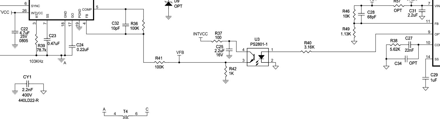
Having a small issue with my power supply design, its a 250-350V to 24V DC-DC forward converter, Basically I was having issues with jittering on my mosfet gate. I changed my compensation network values, this got rid of the jittering I was seeing but now when I increase the input voltage the output voltage decreases, is this because I have over compensated the loop?
 

Sorry for my in-experience, but what do you mean by R ratio and RC breakpoints?
 

Also, attached is the type 2 I am using. However I have calculated, C5 to be 590nF, R2 to be 51K and C4 to be 400nF. I dont know if you can see anything obvious wrong with that from just that

Forward compensation.png
 

For the output filter I have a 330uH inductor and 87uF capacitance, switching frequency at 333kHz 200W output

- - - Updated - - -

I have basically taken Lt's DC1929A and modified it, for the filter I have a half wave recification with a 330uH inductor and 87uF capacitance. The feedback network uses the FOD with the compensation circuitry (FB) components i described previously

Compensation network.pngDC1929A.png

- - - Updated - - -

I have a transformer with a 6:1 ratio with Lmag as 4mH, turns 54:9 and have changed the current sense resistor as well

- - - Updated - - -

Is that enough information?
 

It would appear to be over-compensated causing rectification of AC into a DC offset.

If lowering AC in increases PWM current in transformer inductance that results in a bigger spikes that getting half rectified by the comparator controlled zener Opto resulting in a DC offset with higher spikes. just a guess.

The Opto is unfamiliar to me but is like a precision 2.5V zener switch @2.5V threshold in with regulates the IR LED current with high gain. THe BW is limited to 50kHz which is a built-in breakpoint. which should attenuate most of the spike at 333kHz rep rate, (which may be an issue)

THis makes the transfer function of the FB filter and OPTO combination undefined without input ripple waveforms. Test measurements would help of transfer function for AC and DC.

LED current appears to be 20V/10K=2mA which is lower than what I would use. ( 10 mA )
Thus the input impedance toggles between 10K and open circuit for Opto-pin6 ( half wave rectifier effect on Zin)

DC ratio is 2K/(2K + 16K+ 1.2K) *24V = 2.5V good.

You don't show a plastic cap between iso-gnd and sys-gnd. Careful, although this degrades HV transient isolation, it improves CM noise emission and perhaps differential noise regulation.

The FB filter output impedance on comp network is (2K//17.2K + 590nF (C5))//(R2+C4) into 10K|∞ load.

More test results on transfer function of opto and entire regulator in AC+DC plots and frequency domain will reveal the optimal solution for DC regulation, stability and phase noise..


Also review suggest Comp network transfer functions, may be more linear.
6172630700_1427141237.jpg


Don't forget to verify MOSFET bridge dead-spot duration ~2us or optimize for spikes and shoot-thru then test step load stability over range.

Good luck.
 
As you increase the input volts, this may well increase the RFI noise generated by the switching fets, and this can get into all sorts of places and affect the DC regulation, try 470 ohm resistors directly on pins 4 & 5, if you can, to block the RFI from getting into the chip from the feedback components that can act as good little aerials and pick up such noise...
 
Thanks Sunnyskyguy,

Sorry for all the questions, I wish I had your level of experience.

Test measurements would help of transfer function for AC and DC.

Sorry for the obvious question but what measurements would these be?

THe BW is limited to 50kHz which is a built-in breakpoint. which should attenuate most of the spike at 333kHz rep rate, (which may be an issue)

Why would this cause an issue?

LED current appears to be 20V/10K=2mA which is lower than what I would use. ( 10 mA )

Why would you use 10mA then?

You don't show a plastic cap between iso-gnd and sys-gnd.

Yes your right! I basically removed all of the secondary side components from the demo board and modified my own but have not connected cy1 to my iso-gnd and sys-gnd

Orson cart

try 470 ohm resistors directly on pins 4 & 5
isnt R41 helping with that issue?
 

Every part of the circuit has a function defined by its transfer of voltage, impedance or current.
Since Control Systems are usually modelled by gain of voltage or conversion to this, the stability and DC offset can be corrected by understanding the transfer function.

Like a simple filter or a linear amp or voltage controlled optoisolator.... Try to find test the signal gain and +-DC gain of each block. Eventually when you take control Theory you learn how to analyze instability and correct it.
For now a swept frequency response and Step response will show you. Compensation comes in the form of proportional gain, integral and derivative to adjust phase or modify sensitivity to frequency.

If you aren't worried about pulse to to pulse phase control of the load then 50kHz BW is ok when bulk storage cap can hold voltage long enough while active regulator responds.

Increasing SNR includes increasing LED coupling current to improve feedback SNR. The limiting factor may be lack of AC isolation ( stray leakage of E field or H field ... capacitive or inductive) and thus some coupling from output to input may be distorting the gate drive or gate noise , which was suppressed by rather large coupling cap between sys. and iso gnd.

If you stray from the demo design, make sure you consider the consequences.
 
Thanks again SunnySkyGuy,

You don't fancy a trip over to the UK so I could absorb all of your knowledge, could really do with it :).

Try to find test the signal gain and +-DC gain of each block. Eventually when you take control Theory you learn how to analyze instability and correct it.

I have a frequency response analyser, how would you go about testing each block. I have only have minimum experience in a full loop system testing with the AP300 (linked below), also what would I be looking for?

**broken link removed**

Sometimes it feels like :bang:

Once again thanks for your advice its been invaluable.
 

Also if you are soldering chip caps into the control loop circuit / pcb, worth noting that some are very sensitive to a slodering iron and go leaky (e.g. act like there is a res in parallel) and this can affect the level the DC out settles to.
 

Status
Not open for further replies.

Similar threads

Part and Inventory Search

Welcome to EDABoard.com

Sponsor

Back
Top