Continue to Site

Welcome to EDAboard.com

Welcome to our site! EDAboard.com is an international Electronics Discussion Forum focused on EDA software, circuits, schematics, books, theory, papers, asic, pld, 8051, DSP, Network, RF, Analog Design, PCB, Service Manuals... and a whole lot more! To participate you need to register. Registration is free. Click here to register now.

output voltage swing of two stage fully differential OPAMP

Status
Not open for further replies.

nisha gupta

Member level 4
Joined
May 22, 2012
Messages
71
Helped
0
Reputation
0
Reaction score
0
Trophy points
1,286
Location
Hyderabad, Andhra Pradesh, India
Activity points
1,755
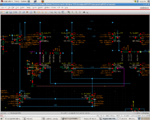
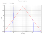
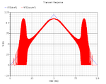
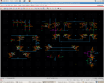
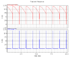
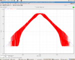
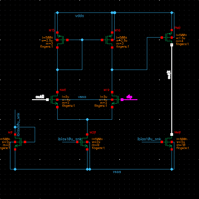
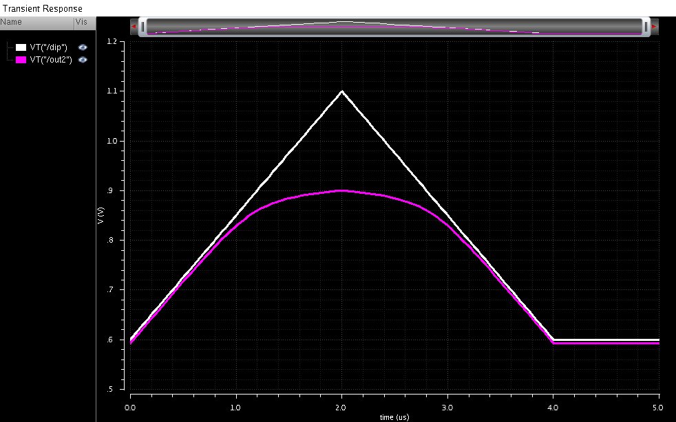
i have designed two stage fully differential OPAMP. i have theoretically calculated output swing, it is coming 172mV to 945mV. power supply is 1.2V in 65nm technology. for checking in voltage swing in simulation i have connected it like a buffer and input sweeped fron 0 to vdd. but output is not tracking input at all. i m attaching plots. plz tell me the region.
 

Attachments

  • analog mosOPAMP.png
    analog mosOPAMP.png
    99 KB · Views: 215
  • ICMR.png
    ICMR.png
    6 KB · Views: 198

Fully differential OPAMPs need CMFB.
 

It looks like you have connected it as some sort of a comparator. Are you sure the feedback is negative?
 

ya feedback is negative........ i m attaching output swing plot and transient plot with RC feedback. plz tell me where i need to do correction.
 

Attachments

  • ICMR with CMFB.png
    ICMR with CMFB.png
    6.8 KB · Views: 152
  • transient.png
    transient.png
    8.3 KB · Views: 153

I cannot recognize if your ac input sources include a DC part. If not, both your inputs (in+, in-) are at vss potential, which surely isn't a good operation point (not in the ICMR).

Moreover, if these input sources actually are 10nA ac current sources without DC current part, they force your outputs to GND potential, too - surely not an OP in the OCMR. With 10nA DC and 3MΩ feedBack resistance (I can't recognize it clearly), it would only be 30mV DC output.

Otherwise, if these input sources were voltage sources, they'd short circuit your feedBack (regarding ac) to GND (vss) potential, so render it inefficient. Your opAmp then would work in open loop.

Means: your test bench setup isn't correct. You have to care for appropriate operation point and correct feedBack by choosing the right DC and ac input values, together with an appropriate input generation resistance for your feedBack.
 

Consider that the absolute output range, and the useful
output range will certainly differ. Once you start to bury
the cascode devices, your Rout and your gain will drop
big-time (as well as your frequency response into any
significant output capacitance, change markedly). The
matching of load and compensation to output capability
and common-mode-position wants some care especially
in low power amps with bare current-source / transconductor
type outputs.
 

I cannot recognize if your ac input sources include a DC part. If not, both your inputs (in+, in-) are at vss potential, which surely isn't a good operation point (not in the ICMR).

Moreover, if these input sources actually are 10nA ac current sources without DC current part, they force your outputs to GND potential, too - surely not an OP in the OCMR. With 10nA DC and 3MΩ feedBack resistance (I can't recognize it clearly), it would only be 30mV DC output.

Otherwise, if these input sources were voltage sources, they'd short circuit your feedBack (regarding ac) to GND (vss) potential, so render it inefficient. Your opAmp then would work in open loop.

Means: your test bench setup isn't correct. You have to care for appropriate operation point and correct feedBack by choosing the right DC and ac input values, together with an appropriate input generation resistance for your feedBack.

hi
thanks for making me clear for input and output.... but i want to clear that 10nA is the ac current which i want to convert in voltage. i m not giving any DC because there is RC feedback so i think no need for DC input.. i can change the amplitude of input current, maximum i can give upto 400mV. because vdd is 1.2 V and feedback resistance is 3K. evenif i have increased to 400mV then also transient output is same.
 

Hi

Can you please do a test case by removing the RC feedback and provide DC for Input and set the Output common mode to 600mV.

After doing this, check with your transcient response. after this , it would be easy to spot the problem.

thanks
 

Hi

Can you please do a test case by removing the RC feedback and provide DC for Input and set the Output common mode to 600mV.

After doing this, check with your transcient response. after this , it would be easy to spot the problem.

thanks

yes i have tested in open loop condition also. in that case transient is perfect and output common mode is 600m. but when i gave sweeped input output is oscillating as shown in attached plot
 

Attachments

  • ICMR.png
    ICMR.png
    67.2 KB · Views: 170

Hi

You are sweeping Vin+ what about your Vin- input and I think this is transcient response of your circuit when you give this triangular pulse.

And measure all the nodes to find why it is happening.. there must be something oscillating in the circuit.
and it takes your vin+ sweep as the common mode and superimposing with that. Please measure the outputs of both nodes.

And I think the input current which is 10nA at 1MHz is causing this .. so remove this source and just give the sweep input with good common mode.

Thanks.
when i m sweeping the input OPAMP is connected as a buffer so vin- is connected to vout+ for checking the output swing. ya this is also kind of transient
if i m giving differential sin at input then transient is perfect.
 

If you want it to be like buffer then you have to use single ended output instead of differential output and give feedback as 180 deg between both inputs. By doing his you can make it track your input.


Or It may be the undamped response of your system. Change the cap size and try again. I will also try that.
 
Last edited:

Actually It is because of Positive feedback you are giving.

So that you are getting the oscillations.

And if you give out- instead of out+ you wont get any oscillations since it is a negative feedback.
 

Actually It is because of Positive feedback you are giving.

So that you are getting the oscillations.

And if you give out- instead of out+ you wont get any oscillations since it is a negative feedback.

Hi
I couldn't understand how it is positive feedback . I have connected in- to out+. Plz explain me.
 

Hi

let us take the phase shifts ok.
1) you are giving input to vin+ and it produces the output on the drain of the NMOS --> which has 180 deg phase shift

2)then this is given to the PMOS where we get the out+ which is another 180 deg.

So phase shift between in+ and Vout+ is 360 deg you are giving this Vout+ to in- so in+ and in- has zero phase difference(because the total phase is 360 deg)

Try it by yourself and you will get what i said..

Thanks

- - - Updated - - -

Hi since it is a NMOS pair opamp it cant give outputs for a wide range. It will give output tracking of VDD/2 to VDD only.

And I attached a modified circuit for DC tracking (to act as a buffer). and attached the output too.

It must be single output opamp to produce DC tracking.


Thanks
 

hi everyone
thanks for helping. now i want to ask question, it may be easy but i got confused. for simulating transimpedande amplifier in close loop i m using differential Isin. so resistance should be in series or parallel with Isin? i need to connect some input resistance because previous circuitry have output impedance.
 

Status
Not open for further replies.

Similar threads

Part and Inventory Search

Welcome to EDABoard.com

Sponsor

Back
Top