Continue to Site

Welcome to EDAboard.com

Welcome to our site! EDAboard.com is an international Electronics Discussion Forum focused on EDA software, circuits, schematics, books, theory, papers, asic, pld, 8051, DSP, Network, RF, Analog Design, PCB, Service Manuals... and a whole lot more! To participate you need to register. Registration is free. Click here to register now.

bfr96s running hot in RF amplifier

Status
Not open for further replies.

neazoi

Advanced Member level 6
Joined
Jan 5, 2008
Messages
4,122
Helped
13
Reputation
26
Reaction score
15
Trophy points
1,318
Location
Greece
Activity points
36,951
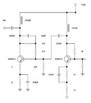
Hi I have made a small HF qrp transmitter (oscillator followed by two bfr96s buffers).
I have not a schematic to show yet but I have found that these class-A (I think) buffers give lowest harmonics (sinewave distortion) at a certain bias point, but they really get hot at that point. Especially the final one get's so hot that it cannot be touched for more than 4-5 seconds with the finger.
The buffers operate at 12v at 170mA in total.
While they get very hot, I do not see problems in the output waveform in neither 50R loadand no problems on open or short-circuit output.

Is that normal for the bfr96s when running in class-A (the same current is drawn efen with no input signal)?
 

Yes, class A is most inefficient and creates highest power dissipation.
What is the voltage across transistor (Vce) ?

 
  • Like
Reactions: neazoi

    neazoi

    Points: 2
    Helpful Answer Positive Rating
2.04W Power dissipation is too much for BFR96S...
100mA max. permissible Ic has been mentioned in its datasheet.typical Ic should be around 70mA.
 
  • Like
Reactions: neazoi

    neazoi

    Points: 2
    Helpful Answer Positive Rating
2.04W Power dissipation is too much for BFR96S...
100mA max. permissible Ic has been mentioned in its datasheet.typical Ic should be around 70mA.

These are the buffers. I measured the current in each of them. the first buffer draws around 40mA at 12v and the second 110mA at 12v.
how does it seem?
 

Attachments

  • amp.JPG
    amp.JPG
    18.1 KB · Views: 225

The last transistor dissipates still 1.32W-0.242W=1.078W that is much.Max. persmissible dissipation is 700mW for BFR96S.
It will be over heat without heatsink no doubt..
 
  • Like
Reactions: neazoi

    neazoi

    Points: 2
    Helpful Answer Positive Rating
The last transistor dissipates still 1.32W-0.242W=1.078W that is much.Max. persmissible dissipation is 700mW for BFR96S.
It will be over heat without heatsink no doubt..

What shall I do? increase the 5R emitter resistors or play with the base bias?
 

What shall I do? increase the 5R emitter resistors or play with the base bias?

In fact, your circuit seems to me a bit weird.Which frequency you work at ??If this circuit is buffer, it should normally have a low output impedance but it doesn't.It consists of 2 cascaded stages and the design has some errors in my opinion.The circuit seems to work at low frequencies like roughly DC-30MHz, if it's so why BFR96S ??? There are millions of transistor that are able to yield this power level and maybe more.I couldn't understand of using BFR96S for this frequency band.This transistor is for wideband applications and I used it 30 years ago.
Could you tell me what your exact intention is ??
 
  • Like
Reactions: neazoi

    neazoi

    Points: 2
    Helpful Answer Positive Rating
In fact, your circuit seems to me a bit weird.Which frequency you work at ??If this circuit is buffer, it should normally have a low output impedance but it doesn't.It consists of 2 cascaded stages and the design has some errors in my opinion.The circuit seems to work at low frequencies like roughly DC-30MHz, if it's so why BFR96S ??? There are millions of transistor that are able to yield this power level and maybe more.I couldn't understand of using BFR96S for this frequency band.This transistor is for wideband applications and I used it 30 years ago.
Could you tell me what your exact intention is ??

Yes, my intention is to make a broadband buffer amplifier from 160-10m without the use of output LPF, so harmonics must be kept low.
My experiments/measurements are all made on 50R but the buffers respond to 1Mohm without noticeable distortion.
I have tried 4:1 transformers without any real difference on the measurements.
BFR96s is only used because it gave me the best power output and the less harmonics (FFT) from the available I had. Anything else to propose?
Any thoughts/improvements would be really appreciated.
 
Last edited:

Find a cheap 2N2222A (1.8W) or 2N2219A (3W) and it will work much better for this application than BFR96.

https://www.farnell.com/datasheets/1449532.pdf

Thanks! I will try them today and let you know.
I have previously tried the PN2222 (plastic version of the 2n2222) for the first buffer and it got very hot, also amplification was not so much and harmonics were a bit higher, if I remember well. Replacing this stage with a bfr96 seemed to solve these problems. But I will try the more powerful 2n2222 or the 2n2219 and let you know.

Do you think that it matters that I do not have a broadband transformer at the output of each stage?
The amplifiers seem to provide the power needed, at the frequencies needed and the distortion levels at 50R, using just chokes. Would I need to care too much about the impedance, since the waveform is very much ok when measured at 50R? After all, antennas are NOT really 50R at all frequencies, try to measure any antenna with an impedance analyzer at different frequencies...
 
Last edited:

What shall I do? increase the 5R emitter resistors or play with the base bias?

To change only DC feedback without changing RF behaviour you can increase the 15 Ohm emitter resistor, instead of the 5 Ohm that also controls the RF feedback.

But why don't you try to increase the 510 Ohm base resistor first?
 
  • Like
Reactions: neazoi

    neazoi

    Points: 2
    Helpful Answer Positive Rating
To change only DC feedback without changing RF behaviour you can increase the 15 Ohm emitter resistor, instead of the 5 Ohm that also controls the RF feedback.

But why don't you try to increase the 510 Ohm base resistor first?

I tried a 6.8R instead of 5R at the emitter, which lowered the gain a bit (but within my specs of 100mW of output power @ 50R). When the oscillator coupling set again so that the output signal from the buffers was 6.3vpp @ 50R (~100mW), the harmonics improved by 1-2db more, so I was pleased to see that.

I do not remember well, but I think I set the 510R by observing the harmonics levels on the FFT. I will try to increase this value to see how it will behave. Will this affect the gain of the transistor or just the bias level?
 

I tried different transistors (about 10-15 available in the lab) with high and lower FTs and Ic>100mA. With these circuit values, only the bfr96s gave this performance (-40dbc harmonics), all others were -30 to -37dbc. I cannot explain why this happens but experimentally it seems true.
However, I have not tested the different transistors and at the same time altering the base resistors. Maybe an optimum point could be found with some of them as well.

Can you specify your targets ?? Frequency,Bandwidth,Output Power,Harmonics' Levels,Gain, etc.
 
  • Like
Reactions: neazoi

    neazoi

    Points: 2
    Helpful Answer Positive Rating
Can you specify your targets ?? Frequency,Bandwidth,Output Power,Harmonics' Levels,Gain, etc.

The goal is to build an easy and cheap broadband QRPp transmitter for HF and the frequency must change by just changing the resonant circuit. It is not easy to accomplish, if no switching (manual or automatic) is to be done. Harmonics (signal distortion) must be kept low at all stages, because no output filtering is used (although not so important in these low power levels, but I want to be compatible with the regulations).
The frequency range must be 1.8-30MHz
The output power is settable by varying the oscillator coupling to the buffers. An output power of 100mW@50R is desirable and in fact I make all the measurements at this output power and impedance, on the FFT, so some absolute error is acceptable.
The oscillator that drives the buffers, outputs around 200-400mVpp@50R and the harmonics of the oscillator operating alone are more than -50dbc.
The first buffer amplifier, outputs 4.2mW@50R for a 100mW@50R out from the final amplifier.
The harmonics must be kept as low as possible, to ensure low distortion of the sinewave. I am doing this because I do not use LPFs at the output, to make the switching between different bands cheaper and easier. The harmonics now are all below -40dbc (which is already a good value?) at all frequencies at 100mW output.

Just a note, I have used 100uH molded chokes, but I have noticed that if I switch to "T" amidon toroids (eg T37-2) harmonics are improved by 1-2db more in some bands, reaching around -43 to -45dbc, but the gain flatness throughout the bands gets worse. Switching to FT types makes no difference. Also changing to broadband toroids (**broken link removed**) does not seem to have any difference to the molded chokes.
 
Last edited:

The frequency range must be 1.8-30MHz
The output power is settable by varying the oscillator coupling to the buffers. An output power of 100mW@50R is desirable and in fact I make all the measurements at this output power and impedance, on the FFT, so some absolute error is acceptable.
The oscillator that drives the buffers, outputs around 200-400mVpp@50R and the harmonics of the oscillator operating alone are more than -50dbc.
The first buffer amplifier, outputs 4.2mW@50R for a 100mW@50R out from the final amplifier.
The harmonics must be kept as low as possible, to ensure low distortion of the sinewave. I am doing this because I do not use LPFs at the output, to make the switching between different bands cheaper and easier. The harmonics now are all below -40dbc (which is already a good value?) at all frequencies at 100mW output.
Briefly..
Output Power=100mW (20dBm) during whole band
Bandwidth=1.8-30MHz
Input Power =( lowest case ) 0.1mW ( -10dBm)
Gain=30dB or slightly more
Input and Output terminations= 50 Ohm

*There will be 2 stages
*Push-Pull configuration ( recommended) will decrease the even order harmonics


I will do something for you, gimme some time...
 
  • Like
Reactions: neazoi

    neazoi

    Points: 2
    Helpful Answer Positive Rating
Briefly..
Output Power=100mW (20dBm) during whole band
Bandwidth=1.8-30MHz
Input Power =( lowest case ) 0.1mW ( -10dBm)
Gain=30dB or slightly more
Input and Output terminations= 50 Ohm

*There will be 2 stages
*Push-Pull configuration ( recommended) will decrease the even order harmonics


I will do something for you, gimme some time...

Thank you I appreciate!
 

Here is a preliminary circuit.You should use 2 identical stages in cascade.
single_stage.png

Gain=42dB
Flatness=0.2dB (1-30MHz)
S11=-25dB or better@50 Ohm
S22=-25dB or better@50 Ohm
P1dB Compression Point=24dBm@30MHz

If you use 10dB-15dB attenuator that will limit the input power upto -20dBm, you'll get very nice Output Spectrum.In this case;

F1=21.7dBm ( F1=30MHz)
2*F1=-49dBc (-27.5dBm)
3*F1=-44.5dBc (-22.8dBm)

It's a very smooth A-Class Linear Amplifier and it consumes approx. 200mA@12V.It might be less of course, you can play around this prototype.
 
If you use Vdd=8V, Power Dissipation over each transistor will be under the limit values.SOT89 is a very nice package that can be easily soldered on a copper heatsink therefore there won't be any particular power dissipation problem with it.In that case of Vdd=8V
HF_Spectrum.pngWaveform.pngHF_Spectrum2.png
 
Here is a preliminary circuit.You should use 2 identical stages in cascade.
View attachment 114756

Gain=42dB
Flatness=0.2dB (1-30MHz)
S11=-25dB or better@50 Ohm
S22=-25dB or better@50 Ohm
P1dB Compression Point=24dBm@30MHz

If you use 10dB-15dB attenuator that will limit the input power upto -20dBm, you'll get very nice Output Spectrum.In this case;

F1=21.7dBm ( F1=30MHz)
2*F1=-49dBc (-27.5dBm)
3*F1=-44.5dBc (-22.8dBm)

It's a very smooth A-Class Linear Amplifier and it consumes approx. 200mA@12V.It might be less of course, you can play around this prototype.

First of all I would like to thank you very much for your time on the design, which I would really like to try and compate to mine!
I first thought that it would be a push pull device, thank god it is a cascaded class-A.
The thing that scares me is the choice of the transistor, it costs 12-15Euros each one on ebay (inc. pp)! That is too much, I wonded if an alternative could be used.
 
Last edited:

Status
Not open for further replies.

Part and Inventory Search

Welcome to EDABoard.com

Sponsor

Back
Top