Continue to Site

Welcome to EDAboard.com

Welcome to our site! EDAboard.com is an international Electronics Discussion Forum focused on EDA software, circuits, schematics, books, theory, papers, asic, pld, 8051, DSP, Network, RF, Analog Design, PCB, Service Manuals... and a whole lot more! To participate you need to register. Registration is free. Click here to register now.

Help need for difficulties while Drawing Diagrams Using KiCAD software

Status
Not open for further replies.

raju_kambar

Full Member level 3
Joined
Jun 19, 2013
Messages
153
Helped
5
Reputation
10
Reaction score
5
Trophy points
18
Location
Earth
Activity points
1,404
Dear Sir,
I am using KiCADsoftware for drawing my Electronic Circuit Diagrams. I am facing following problems while drawing my circuit diagrams using KiCAD software.

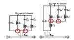
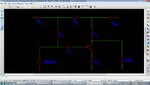
(1) While naming for components such inductors (L), capacitors(C), and Resistors(R). I know how to change the size of the Text. I don't know How to change the " TEXT" for the desired "font style" such as TIMES NEW ROMAN or CALIBRA or TAHOMA etc.... Can you help me to get change the "TEXT" to the desired "font style"(Example Screen shot is shown in Diagram_For_TEXT_and_Junction_ Require_Change)

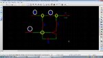
(2) If two are components connecting using some wires and forming "JUNCTION" with another component. How to highlight this " JUNCTION" with Bigger size. Presently if we drag and place the "junction" it is not visible . How to make visible junction connecting using "JUNCTION" symbol . I need the junction points as like screen shot shown in figure (Name Junction_Point_Highlighter_Figure).

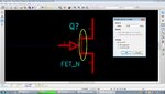
(3) I want to change the line width of the components such as transistors. For changing transistor each line width I am going right click on the component, and then select the "Edit Component" and clicking on the desired lines to change using "Edit line options" and go to File and save current library. Line width are changing as changes the "Edit line options". But When I came back to schematic changed line effect is not visible in the schematic window. How to get effect of changing the line width in the schematic, when we change in the "edit line options" ( Example Screen Shot is shown in the FET_N_LINE_WIDTH_CHANGE)
(4) When we are making changes to present library available components and how to save it permanently to frequently use with another name and make it utilize in the future.
Can you anybody help me to resolve the above difficulties.
 

Attachments

  • Junction_Point_Highligter_Figure.jpg
    Junction_Point_Highligter_Figure.jpg
    31.4 KB · Views: 153
  • Diagram_FOR_TEXT_and_Junction_Require_Change.jpg
    Diagram_FOR_TEXT_and_Junction_Require_Change.jpg
    247.9 KB · Views: 153
  • FET_N_LINE_WIDTH_CHANGE.jpg
    FET_N_LINE_WIDTH_CHANGE.jpg
    162 KB · Views: 148

Some can try to solve my difficulties in the posting #1.
 

Is not possible change desired font style as TIMES NEW ROMAN Or CALIBRA or TAMOHA for " TEXT" in the KiCAD software while drawing electronic schematic circuits and also not possible to make the junction as like posting # 1 junction_point_highligter_figure screen shot showed.
Can you clarify it.
 

You are asking for something that is unusual and to my best knowledge, is not a feature of any CAD package. They all try to make schematics as clear and detailed as possible but you are requesting 'fatter' wires, junctions and symbols. That will inevitably mean less detail and limit the complexity of a design on the page. I have already explained how to edit symbols and wire thickness on an individual basis, for clarity of purpose sometimes this is something a designer might want to do.

KiCad is a first class CAD package and excellent for schematic and PCB design but if you need something for making big pictures, a graphics package would be more suitable.

Alternatively, you could try printing the schematic to a file and post-editing it with a graphics package but I can't advise on which may be suitable.

Brian.
 
I have already explained how to edit symbols and wire thickness on an individual basis, for clarity of purpose sometimes this is something a designer might want to do.
KiCad is a first class CAD package and excellent for schematic and PCB design but if you need something for making big pictures, a graphics package would be more suitable.
Alternatively, you could try printing the schematic to a file and post-editing it with a graphics package but I can't advise on which may be suitable.
Brian.
Dear Sir,
You have helped like anything earlier, you have cleared my all doubts. I am very much grateful to you. KiCAD is very good software, there is doubt it.

I need the following modification while creating Schematic using KiCAD software

(1) I need all the "TEXT" in the schematic to convert those into desired font style such TIMES NEW ROMAN or CALIBRA or TAHOMA .....etc. Presently it allowing to do normal or Bold or Bold italic or Italic with "TEXT" size we can change. How to convert the "TEXT" into a desired font Style.
(2) Three wires connecting at the same point. Junction will form. I have to highlight the junction even all three wires are "fatter". Now junction is showing for the thinner three wires are meeting at the same point.
(3) In my schematic, I have set the "line width" using preferences -> options -> Line width , but all "line width"s are not appearing similar line widths. Some are appearing more thicker than other. I want to get look all line widths in the schematic same thickness.
Below I have shown the screen shot of printed Schematic generated from KiCAD and also screen shot of KiCAD schematic is showed.
 

Attachments

  • Prnted_ Schematic_Using_KiCAD.jpg
    Prnted_ Schematic_Using_KiCAD.jpg
    55.7 KB · Views: 156
  • Schematic_Drawn_Using_KiCAD.jpg
    Schematic_Drawn_Using_KiCAD.jpg
    252.7 KB · Views: 163

I think the fonts are embedded in Kicad, if you changed them the text may no longer fit the part outlines in the schematic or PCB silk screen.

The line widths may be a rounding error in the conversion to a graphic image format, I do not see it on my computer.

As for connecting dots, I would guess they are also embedded in the program as they are not 'symbols' in the sense of component outlines.

As I stressed, what you ask for is not normal in CAD packages but I suggest for more advice you look at the "Kicad_users" group on Yahoo Groups where most Kicad users and developers hang out.

Brian.
 

What I can figure of what is being asked for is perfectly normal in professional CAD packages?

1) Changing text size & font.
2) Defining junction size.
3) Changing Symbol line width.

All easily changeable in CADSTAR and I'd expect other CAD packages to be able to do this.
Looking at the above schematics, perhaps there is not junction because they are not actually connected correctly?

RE changing the text font - a Google search shows me plenty of posts where others are asking the same and the developers are talking among themselves saying it's hard to do.
And after downloading the latest release I can see where the OP's problem is - there is no way to do this.
It seems the software writers have not enabled it to use anything other than the system font yet (I see complaints of how hard it is to do so, yet other packages can use TTF fonts).

Looking at the demo schematic I can see good sized junctions - this to me IS suggesting that his connections are not fully made.

To change the line width of the transistor - RMB and select"Edit Component - then "Edit with Library Editor".
Then RMB on the line and select "Edit Line Options" and type in your chosen width.
When happy use "File\Save Library" and it will be updated on the schematic.

For the font - It think your stuck with it, but that's the sort of thing you get with free programs - very little flexibility.
I certainly would NOT call this first class.
 
Last edited:
All the things that the OP wanted can be easily done in proteus. But if you have invested much time is using KiCad, I doubt it is beneficial to switch to another package and start from new.

Maybe you can download the free demo version of proteus 7.xx and have a test drive to see if you like it. Is there a paid version of KiCad with more functionalities that you can try on?

Allen
 
I think it's more a case of learn how to use it correctly and lower his expectations from a free program. ;)
 
I use Kicad extensively and it's fine when used as intended. What Raju_kambar wants is a way to 'beef up' all the lines, symbols, text and junctions without enlarging the size of the diagram. It would be rather like using 'bold' font instead of 'normal' but on all the entities in the diagram, not just text. Text in Kicad can already be in any of the standard font variations but the underlying font itself is fixed. To me, the obvious solution is to enlarge the image, maybe breaking it into smaller sections if it overflows a page but simply making everything fatter will inevitably fill in the spaces in symbols and text, making it less readable.

Incidentally, the latest release number for the Windows version is 5376 and Raju is using (I think) version 4022 which is about 18 months out of date.

Brian.
 
Status
Not open for further replies.

Part and Inventory Search

Welcome to EDABoard.com

Sponsor

Back
Top