Continue to Site

Welcome to EDAboard.com

Welcome to our site! EDAboard.com is an international Electronics Discussion Forum focused on EDA software, circuits, schematics, books, theory, papers, asic, pld, 8051, DSP, Network, RF, Analog Design, PCB, Service Manuals... and a whole lot more! To participate you need to register. Registration is free. Click here to register now.

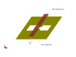
3D layout of Defected Ground Structure

Status
Not open for further replies.
ADS like other electronic layout design tool has a 3D circuit viewer.

dgs.png
 
  • Like
Reactions: zeshan1701

    V

    Points: 2
    Helpful Answer Positive Rating

    zeshan1701

    Points: 2
    Helpful Answer Positive Rating
Dear RealAEL, first of all thanks for your reply. Can you please guide me how to put annotations on such a type of layout.
 

File > Save Image... (for png, jpg, tiff or gif formats) then read into Powerpoint (or any similar editing software) and add annotation as required. Save as original format when done.

dgsa.png
 
maybe HFSS or CST can do this easier.
 

This can be done in AWR/Microwave Office. Define the DGS structure as a negative layer.
 

Status
Not open for further replies.

Part and Inventory Search

Welcome to EDABoard.com

Sponsor

Back
Top