Continue to Site

Welcome to EDAboard.com

Welcome to our site! EDAboard.com is an international Electronics Discussion Forum focused on EDA software, circuits, schematics, books, theory, papers, asic, pld, 8051, DSP, Network, RF, Analog Design, PCB, Service Manuals... and a whole lot more! To participate you need to register. Registration is free. Click here to register now.

[SOLVED] Pure sinewave inverter with toroidal transformer

Status
Not open for further replies.
Yes, having minimal dead time reduces the amount of charge carriers picked up by the internal diode, with the internal mosfet shorting the internal diode these diodes aren't fully off (junction swept of charge and reversed biased) when hit by the other fet turning on.... depending on how fast you are switching some small snubbers will help get the spike down, say 330pF and 33 ohm across each fet as a starting point...

- - - Updated - - -

Actually a slightly faster turn on of your upper devices may help if it shortens the dead time....

- - - Updated - - -

Sorry that should be 2.2nF (1kV) and 10 ohm (2W) across each fet...
 

    V

    Points: 2
    Helpful Answer Positive Rating
Hello everyone
Pla how does one calculate how many MOSFET will be needed for an full bridge inverter using N channel MOSFET.
If I have irfp260n having power at 300w then using four of it in the bridge will give how much power output assuming no losses. Basically how to calculate number of MOSFETs needed depending on power output.
 

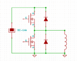
During normal operation (unipolar PWM scheme), the H-bridge looks like that (transformer primary tied to GND):

h-bridge.gif

Am I wrong, or just the low-side diode it's freewheeling? (the inductor current flows from DC bus to GND)

I am asking this because I want to put external Schottky diodes across MOSFETs but seems to me like only the low-side ones need that.

Speaking of that, I wonder what type of connection (PCB trace, twisted wires, thick wire) to use for placing those external Schottky diodes across MOSFETs (actually, across the switching node and GND). The distance between connecting pads it's about 6cm.
 

In terms of stray inductance, 6 cm is light years away. The Mosfet's body diodes will have already begun conducting, before the stray inductance allows the schottkys to start conducting.

Can you solder the diodes across the Drain-Source terminals instead? And cut the diode's terminals as short as possible.
 

    V

    Points: 2
    Helpful Answer Positive Rating
My intention is to mount them on a heatsink (they come in TO247 package).

I don't mind if the body diodes start conducting first as long as the Schottky ones do the same thing (even after a short delay).

Having a lower forward voltage, they should bypass the body diodes thus will deny any recovery charge accumulation in those body diodes. That means there will be no reverse recovery process neither (to generate that overshoot).
 

The TO247 package has sufficient space to solder a SOD123-packaged diode directly across the D-S legs.
 

To make myself clear: the Scottky diodes (IR 60CPQ150) come in TO247 package (dual common cathode) and I want to use two of them in parallel (for a total of 4 x 30A rated current), mounted on a small heatsink.

Actually, the MOSFETs came in TO247 package too but I've mounted them (4 in parallel for every switch) on a separate/bigger heatsink and I can't solder the Schottky diodes right across them.

That's it, I'll mount those diodes on a small PCB and I'll check the results.
 
Status
Not open for further replies.

Similar threads

Part and Inventory Search

Welcome to EDABoard.com

Sponsor

Back
Top