Continue to Site

Welcome to EDAboard.com

Welcome to our site! EDAboard.com is an international Electronics Discussion Forum focused on EDA software, circuits, schematics, books, theory, papers, asic, pld, 8051, DSP, Network, RF, Analog Design, PCB, Service Manuals... and a whole lot more! To participate you need to register. Registration is free. Click here to register now.

[SOLVED] Calculate values in an amplifier

Status
Not open for further replies.

Hatmpatn

Member level 3
Joined
Sep 15, 2014
Messages
59
Helped
0
Reputation
0
Reaction score
0
Trophy points
6
Activity points
515
Good evening all edaboarders!

I've been given a task where I should calculate some values in an amplifier. I have under some time now gathered some knowledge in the electronics area, but not sufficient to solve this problem on my own. I was wondering if you could help me and point me in the right direction, calculations-wise!

Thanks in advance!

The problem:
----------------------------------------------
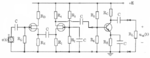
The amplifier has a common-drain amplifier at the input, followed by a common-gate amplifier and finally a common-emitter amplifier on the output.

The values for the resistors are: RD: 2kΩ RS: 15kΩ RG: 1MΩ R2: 16kΩ R5: 40kΩ R6: 10kΩ RC: 3kΩ RE: 2kΩ RL: 2kΩ E=12V

The parameters of the FET-transistors:
Up: -3.5V IDSS: 9mA Slope: 4mS exiting-admittance: 10µS Zin= ∞
This applies to the FET-transistors: iD=IDSS*(1-uGS/Up

The parameters of the bipolar transistor:
In-impedance: 1.5kΩ Feedback ratio: 2*10^-4 Current amplification factor: 100 Out-impedance: 50µS. B=100

uppg3.png

These are the tasks of the problem:

a) Calculate R1, R3 and R4 so that the FET-transistors in the common-gate amplifier gets the operating point IDQ= 4mA, UDSQ= 2V and the gatepotential +2V.

b) Draw an equivalent small-signal schedule for the amplifierm where the FET-transistor's out-admittance and the bipolar transistor's feedback ratio and out-admittance are neglected. The capacitances are great.

Then calculate the out-voltage uout(t) if e(t)=sin(10³t) [mV].
-------------------------------------------------------------------

**Note that I'm not certain of these equivalent words in english which I have translated from swedish.
 

NOBODY makes an amplifier like that except a teacher. Is this homework?
The common-gate FET is not needed and the common-emitter transistor has no negative feedback so its output will be extremely distorted.
 

Yes, this is homework for a introduction course in electronics. Is this a problem?
 

The two FETS are like a long tail amplifier, The current change through the first FET, is split via Rd and R1 (no value) and then flows through R4// input Z of the transistor and R5 and R6 in parallel. So input Z of transistor is Hfe X 25/Ic(mA). The output voltage is the change of Ic X Rc //Rl // output Z of transistor. Ic = Hfe X Ib.
Should get you going?
Frank
 
Do a step at a time. You are given R2 = 16k; what must R3 be for the gate voltage to be 2V, given that E=12V?

Once you have that, what must R1 be for IDQ to be 4 mA?
 
Maybe the teacher wants the student to show that the circuit is wrong?

I re-drew the circuit for it to show the common-drain left FET driving the common-gate right FET.
The FETs are drawn as Jfets which are usually depletion-mode so the source voltage must be higher than the gate voltage for it to be linear.

Then the left Jfet is biased correctly with the gate at 0V and the drain-source current causing a positive source voltage in Rs. But the right Jfet is not biased correctly since its gate is at a positive voltage.
Therefore I think R3 should be removed.

But the circuit does not need two Jfets, a single common source Jfet will replace them and still provide the very high input resistance.
 

Attachments

  • amplifier.png
    amplifier.png
    69.2 KB · Views: 115
Not sure I agree Audioguru,
provided the voltage dropped across R1 is smaller then 2V the bias conditions will be correct, and as Idss is given as 9mA and we are looking for a running cureent of 4mA with pinch off at -3.5V.... some trivial algebra will give the answer for a value of R1, which will indeed be dropping less then 2V.

Once you know the source voltage you know the drain voltage because you can simply add UDS, then as you know the current you can figure out the value of the load resistor R4.

A couple of hints for the second part::
For an AC analysis, caps become short circuits, and the power and ground rails are connected together.
Note that this puts R1 & RS in parallel, this parallel combination is the load for the input fet.

It is the sort of circuit only a teacher could love, if I designed that I would quite rightly be shown the door.

Regards, Dan.
 
There may be doubts if the topology is first choice, but a common gate stage is at least an option for JFET RF amplifiers due to it's low s12. I remember to have used a single JFET CG stage as a VHF antenna preamplifier for my first TV.

The CG stage definitely serves a purpose by increasing the total gain.

The positive gate voltage makes the bias point less sensitive to Vgs,off variations.
 
Since the gate must be +2V then a depletion-mode Jfet needs to have its source at a higher voltage of about 3.5V. Then the value of R1 is 3.5V/4mA= 910 ohms. The load is the base-emitter impedance of the transistor which is about 2.8k ohms so the common-gate Jfet will barely have any gain being loaded down like that.

I guess the teacher bought a few thousand Jfets, measured them all then selected the one with the parameters in the first post here.
It was probably a 2N5459 that has a pinch-off voltage of 2V to 6V and an IDSS of 4mA to 16mA.
 
Whoops you are right, but the win with the common gate may be its very good reverse isolation rather then gain in the usual sense.

If you are having to IDSS and Pinchoff bin jfets for a simple low frequency amplifier then you are doing it wrong.....

Regards, Dan.
 
Since the gate must be +2V then a depletion-mode Jfet needs to have its source at a higher voltage of about 3.5V. Then the value of R1 is 3.5V/4mA= 910 ohms. The load is the base-emitter impedance of the transistor which is about 2.8k ohms so the common-gate Jfet will barely have any gain being loaded down like that.
Vgs according to the assumed JFET characteristic is 1.16 V, so R1 should be 793 (820) ohms. CG input impedance is considerably lower, about 295 ohms. In so far R1 is not the dominant load part for the input stage, but it further reduces the overall gain.

The main reason for low circuit gain is however the low operation current and respectively low gm and high output impedance of the first stage.

A rough hand calculation gives an overall voltage gain of about 0.5. So your basic classification as effectively useless amplifier circuit can be confirmed. The designer managned to add a transistor and reduce the overall gain.
 
Thanks to everyone for showing such great interest in this thread, although you lost me abit in the latest comment.

Listening to The Electrician, I get R3=10V/125µA=80kΩ.

Here's a schedule with the known values.

uppg3värden.png
 

Thanks to everyone for showing such great interest in this thread, although you lost me abit in the latest comment.

Listening to The Electrician, I get R3=10V/125µA=80kΩ.

Here's a schedule with the known values.

View attachment 110591

You are given the transfer characteristic of the FET:

ID=IDSS*(1-UGS/Up)²

What must UGS be to give ID = .004 A?

UG (with respect to ground) is 2V due to the R3R2 voltage divider, so what must be the voltage US (source voltage with respect to ground) so that UGS is what was calculated just above?

Then, what must be the value of R1 (which is carrying .004 A) to give that voltage US?
 
With the given values; Up=-3.5V IDSS=9mA and ID=0.004A

UGS=(1-√(ID/IDSS))Up

Gives UGS=-1.16667V

Should give us US=2V-UGS => US=3.16667V

And with ohms law 3.16667/0.004=791.6675Ω
 

Since R4 is also carrying .004 A, what must its value be so that UDSQ = 2 V?

While you're at it, calculate the transconductance (gm) of the FET with the calculated UGS. This will be the slope of the curve given by iD=IDSS*(1-uGS/Up)²
 
Is it correct to assume that the value for R4 should be 10/0.004=2500Ω?

Just looking briefly at what transconductance is the formula for it is gm=Iout/Vin, this should result in: UGS=Vin=-1.16667V IDQ=Iout=0.004A => 0.004/-1.16667=-3.4286mS

Here's the schedule sofar, not assuming R4 is correct yet.

uppg3värden.png
 

Is it correct to assume that the value for R4 should be 10/0.004=2500Ω?
Where did you get 10 V voltage drop at R4? You want Vds = 2V, not Vd = 2V.

You have Vg = 2V Vs = 3.167 V and Vds should be 2 V. So Vd = 5.167.
 
Is it correct to assume that the value for R4 should be 10/0.004=2500Ω?

No. You want R4 to drop the difference between the 12 volt supply and the voltage on the drain of the FET.

Just looking briefly at what transconductance is the formula for it is gm=Iout/Vin, this should result in: UGS=Vin=-1.16667V IDQ=Iout=0.004A => 0.004/-1.16667=-3.4286mS

You have calculated the DC transconductance (GM). We want the transconductance for small AC signals. The convention is to use lower case for small signal variables, so the formula would be gm = iout/vin. What you must do is take the derivative of the transfer characteristic with respect to the gate to source voltage (ugs) and evaluate that at the gate-source voltage.

By an amazing coincidence, the value of GM is the same as gm at a gate-source voltage of 1.166667 volts! It's not the same at any other (useful) voltage!

You will also need to calculate the gm of the first FET, using the derivative of the transfer characteristic. You will need to calculate the operating point of the first FET to use in the calculation of its gm.
 
Last edited:

Status
Not open for further replies.

Part and Inventory Search

Welcome to EDABoard.com

Sponsor

Back
Top