Continue to Site

Welcome to EDAboard.com

Welcome to our site! EDAboard.com is an international Electronics Discussion Forum focused on EDA software, circuits, schematics, books, theory, papers, asic, pld, 8051, DSP, Network, RF, Analog Design, PCB, Service Manuals... and a whole lot more! To participate you need to register. Registration is free. Click here to register now.

Queries on Simualted and measured Biasing Values of LNA design in ADS

Status
Not open for further replies.
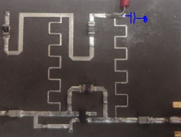
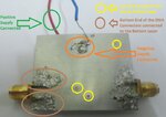
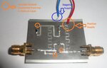
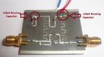
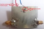
In your PCB, there is one obvious mistake: you do not have any capacitor to ground at the voltage supply lines (meander). Add something like 100pF to ground at the DC supply (if the meander lines are 1/4 wavelength lines: at the DC side of each meander).

Let me repeat this ... independent of your bias problem, your circuit (layout) is not complete. In simulation the 3V supply is an ideal short circuit for RF signals ... but in your hardware it is not. You really need to add a blocking capacitor.
 
your circuit (layout) is not complete. In simulation the 3V supply is an ideal short circuit for RF signals ... but in your hardware it is not. You really need to add a blocking capacitor
Sir,
I agree your suggestion,now already PCB is designed, I have only option of changing the existing components. How can I add blocking capacitors (100pF) on either side of the meander lines. How can I connect externally blocking capacitors on either side of the DC supply meander lines to already designed PCB.
Now it is difficult to add either side blocking capacitors to my existing board, but I have 100pF capacitors.
 

How can I connect externally blocking capacitors on either side of the DC supply meander lines to already designed PCB.

Start with one capacitor, and place it at the meander where you connect the red wire. Drill a small hole and connect the other terminal of the capacitor to the backside ground metal (backside of PCB).

1564247600_1411056317.jpg
 
Sir,
Herewith I attached screen shot of Board

What is that ??
Listen..
A RF PCB or any kind of RF-Microwave circuit is completely different than ordinary circuits.
You circuit was probabaly oscillating in everywhere.There is neither decopuling capacitor, nor applied RF rules,nor GND islands for supply decoupling etc..
Try to make a better one by listening the suggestions of the exprienced guys here..
 
On the topic of ground where is the ground connection for this amp assembly? I can see the red wire for the +ve supply at the top but there doesn't appear to be any ground wire. The only ground connection that is visible is that you would get through the SMA connectors when they are attached to other equipment in your measurement setup provided they themselves were rigidly connected to the ground plane material on the back of the board. Are these connected? This is definitely not a good idea. The ground plane of this amp requires a direct connection to a good ground reference, usually on the DC power supply itself.

Only then can you think about top side ground planes, supply decoupling capacitors, etc.
 
There are many app. notes on its product page.Look at them and inspire from their layouts..
 
On the topic of ground where is the ground connection for this amp assembly? I can see the red wire for the +ve supply at the top but there doesn't appear to be any ground wire.
RealAEL Sir,
Yes , I have connected the ground wire at the bottom layer(it is shown in the screen shot of bottom layer of PCB), BLUE wire shows the ground connection.
The only ground connection that is visible is that you would get through the SMA connectors when they are attached to other equipment in your measurement setup provided they themselves were rigidly connected to the ground plane material on the back of the board. Are these connected?
RealAEL Sir,
Yes, SMA Connectors are connected to ground plane back of the board.
The ground plane of this amp requires a direct connection to a good ground reference, usually on the DC power supply itself.Only then can you think about top side ground planes, supply decoupling capacitors, etc.
RealAEL Sir,
I didn't understand , what you said above, What is this supply decoupling capacitors, I didn't understand, can you make it clear.

I made mistake of not connecting "blocking capacitors" on either side of the meander line DC supply, no problem I will connect the blocking capacitors on either side of the meander line DC supply.
I have shown the screen shots of top and bottom side of PCB. If I made any mistake in the top and bottom side of the PCB, point it out me, I will correct my mistakes. I request you to point my mistakes, if there is mistakes in the top and bottom side of PCB.
 

Attachments

  • Bottom_Layer_Of_PCB.jpg
    Bottom_Layer_Of_PCB.jpg
    84.9 KB · Views: 67
  • Top_Layer_Of_PCB.jpg
    Top_Layer_Of_PCB.jpg
    86.8 KB · Views: 64

Sir,
I am sorry, even I connected the DC blocking capacitors 100pF on either side of meander line DC supply lines. It is showing same biasing as same earlier, it is showing -548mV or "0 V" at the Vgs and Drain current is "0mA".
Screen shots of top layer and bottom layer is shown below.
 

Attachments

  • TOP_Layer_Of_PCB.jpg
    TOP_Layer_Of_PCB.jpg
    70 KB · Views: 61
  • Bottom_Layer_Of_PCB.jpg
    Bottom_Layer_Of_PCB.jpg
    81 KB · Views: 52

In the picture, it seems that you a thin wire from the +3V wire to the ground via at the capacitor, shorting the 3V.

Please show in the picture where (at which point) you measure the voltage.
 
In the picture, it seems that you a thin wire from the +3V wire to the ground via at the capacitor, shorting the 3V.

Please show in the picture where (at which point) you measure the voltage.
Sir,
No, it is not shorted, it seems as shorted,but it is not shorted(Different screen shots is shown, in that you can notice, there is no short)
I have shown in the screen shot, where I am measuring Vgs. At gate of the transistor itself, voltage is showing -567.5mV or 0 Volts sometimes, when 3v supply is on.
 

Attachments

  • Top_Layer_Of_PCB.jpg
    Top_Layer_Of_PCB.jpg
    89.5 KB · Views: 58

Sir,
No, it is not shorted, it seems as shorted,but it is not shorted(Different screen shots is shown, in that you can notice, there is no short)
I have shown in the screen shot, where I am measuring Vgs. At gate of the transistor itself, voltage is showing -567.5mV or 0 Volts sometimes, when 3v supply is on.
Your circuit is oscillating and it disturbs the DMM.
Therefore you read inconsistent values.Chuck out that board and redesign carefully by inspecting the sample boards in app. notes.
That boards will always oscillate, you cannot cut off that.This is my last message..
 

I have shown in the screen shot, where I am measuring Vgs.

That's wrong! Don't do this! Do NOT measure directly at the transitor, because your measurement cable changes the RF behaviour! Measure at the end of the meander line, where you have the blocking capacitor.

- - - Updated - - -

That boards will always oscillate, you cannot cut off that.This is my last message..

You're late, my friend ;-)

You might have missed that pusparaga's design efforts (and questions, questions, questions) are going on for months here, and in other forums. he has real difficulty to understand what he is doing, and there seems to be no supervisors at his university to teach students. Very difficult situation.

His layout has been simulated already (other threads) and it is microstrip only (no extra copper pour), which is ok. Not the nicest layout, but it seems to have worked in simulations, so he can give it a try. The one issue with the blocking caps (not required in ADS because ideal DC source shorts any RF) is beeing fixed.

Let's see what he comes up with.
 

I forgot to mention that you should measure with 50 ohm source and load connected to the LNA.
 

Status
Not open for further replies.

Part and Inventory Search

Welcome to EDABoard.com

Sponsor

Back
Top