Welcome to our site! EDAboard.com is an international Electronics Discussion Forum focused on EDA software, circuits, schematics, books, theory, papers, asic, pld, 8051, DSP, Network, RF, Analog Design, PCB, Service Manuals... and a whole lot more! To participate you need to register. Registration is free. Click here to register now.
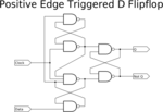
In the above circuit if clock(CLK 1) goes from 0 to 1 and input D =0 ,this makes Q=0.
It is stated that when the clock is at HIGH(1) any further change in input does not affect output,how it is so .Can you explain me please.Thank you in advance
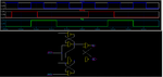
As said, would be necessary perform some analysis step by step, or even simulate. The waveform bellow confirms that the circuit is really not sensitive to changes at DATA pin while CLK stay high.
This site uses cookies to help personalise content, tailor your experience and to keep you logged in if you register.
By continuing to use this site, you are consenting to our use of cookies.