Continue to Site

Welcome to EDAboard.com

Welcome to our site! EDAboard.com is an international Electronics Discussion Forum focused on EDA software, circuits, schematics, books, theory, papers, asic, pld, 8051, DSP, Network, RF, Analog Design, PCB, Service Manuals... and a whole lot more! To participate you need to register. Registration is free. Click here to register now.

Increase linear range of difference differential amplifier with class AB output

Status
Not open for further replies.

Vlad Cretu

Newbie level 6
Joined
Jul 12, 2014
Messages
14
Helped
0
Reputation
0
Reaction score
0
Trophy points
1,281
Activity points
1,385
Hello,

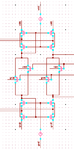
I have rail to rail input diff pair, but I have a 100mV linear range (plotted the derivative of the currents in function of input voltage);

Could you please help with some advice on how to increase this linear range. What is more peculiar is that it's that small with tail to rail input.

Regards,
vlad
 

How do You check this linear range? This DDA works in any closed loop configuration?
 

Show what you have , schematic, parts, layout, signals, pulse bandwidth.

Do U mean crossover distortion range, common mode input range (which you say is Rail-Rail input) or differential input range, which is dependant on gain and output signal?
 

I attached images with results, testbench, full circuit.
I am doing deriv( current from one res + current from the other)
plot the 2 gms as you can see in the image. What i also don't understand is why the gm is the same for both gms. i would expect to see one offseted towards the left and the other on the right.

1.PNG
2.PNG
3.PNG
4.PNG
5.PNG

Also yes it works as expected. The noise is a bit too big though.
7.PNG
2.PNG

Thank you all for the help!
 

Hi Vlad

I am not familiar with the exact circuit you are designing, still in general the input linear range depends mostly on the inversion coefficient of the input pair: it is minimum in weak inversion and grows significantly as you move into stronger inversion.

I am guessing your bias currents are small, what are the Vgs-Vth values for your input pairs?

Increasing the level of inversion of your input pair sadly will not be beneficial to your noise levels

Finally the variable you are calling vcm seems to be equal to half the differential input voltage while the name suggests a common mode voltage... (hopefully nothing more than an unfortunate naming choice)

Hope this helps
 
Why is your schematic a negative with a black background?
Why is it covered in dots?

I converted part of your schematic so it has a normal white background but I could not remove all the dots.
 

Attachments

  • schematic.png
    schematic.png
    6.7 KB · Views: 144

Dear Audioguru

what to you does not look like a "normal" schematic is the de-facto standard for IC design engineers, it is called Cadence Composer and you don't want to know how much a year of license maintenance costs, much less what the initial license cost is...

I don't think the blackgound should be an issue (unless you are trying to print it) but I agree the dots are annoying, they can be easily suppressed before exporting the image and it is a good recommendation

Cheers

Why is your schematic a negative with a black background?
Why is it covered in dots?

I converted part of your schematic so it has a normal white background but I could not remove all the dots.
 

Hello,

They are in saturation slightly :); Vgs-Vth is just a couple of mV. But increasing the biasing current, not only has an impact on my noise, but as well on the power consumption. Which i want to keep to a minimum.

I have an impression that what i measure is the common mode input range. What should i change to measure differential input range? I'm quite lost with the test benching.

Thank you.

Regards,
Vlad
 
Last edited:

Why is your schematic a negative with a black background?
Why is it covered in dots?

As dgnani explained, it's the familiar look and feel of a popular IC design tool. In my view, more annoying than the display style is the fact that Cadence schematics posted at Edaborad are often hiding all or at least many essential design parameters (transistor parameters, resistor values) so that they don't show much more than the bare circuit topology. Respectively no question can be answered without additional informations.

The present forum structure is so that both circuit related IC design questions as well as dicrete analog design problems will go to the "Analog Circuit Design" forum. May be they should be separated into different forums. We already have the "Analog IC Design and Layout" forum, but it focusses on layout and technology rather than circuit aspects.

At present, you should probably ignore posts with the characteristic black screen dumps, at least if you aren't interested to help with the homework of analog IC design classes.
 

1.PNG

This is the most decent level of detail. I don't see why you would want to remove the dots or why does the black bother you. It's in the end just a schematic.

Suggestions regarding the actual problem that I have would be most appreciated.

Regards,
Vlad
 

Hi Vlad. If You are looking for current flowing through resistors, modulated by changing the voltage on fet gates, You shouldn't expect any linear relation. The drain current is described as Lambert W function of Vgs (in first approximation). To check the linear input range of your FDDA, You should connect it as voltage follower (in fact I know how to do this in fully differential option not single ended, but it shouldn't be hard ;-) ) and check relationship between Vout and (Vin+,Vin-).
 
With linearr range you are referring to differential voltage? SunnySkyguy already asked but you didn't answer the question.

The amplifier has no internal feedback (e.g. source degeneration), so the linear input range is small and the linearity low. It will be usually operated with external feedback in a closed loop, ast mentioned in post #2.
 
I spend a few minutes to check DDA operation (but not with rail-to-rail input) and I obtain this results with presented testbench (dda working as inverting followeer)
dda_sim.png
The dc OPs and dimensions are below:
dda_dcOP.pngdda_dims.png

The linear range is below one volt due to input pair limitation and some current balance, but from point of view of your circuit I propose to check it in the same configuration.
 
Hello Dominik,

I have tried replicating your results, however I obtain a smaller range ~380 mV. I double checked, however the results differ.
Also you have MP8 and MP10 not biased. Why did you do that?

In the image I attached what I get using my topology, but with the test proposed by you.
How do you plot the loop gain and phase as you did?
1.PNG

Yes, I would like to find the differential voltage linear range.

Thank you
 
Last edited:

Also you have MP8 and MP10 not biased. Why did you do that?
Oh shit.... I didn't notice that, it could be explain many things ;-) Of course the gates of MP8 and MP10 should be connected together with gates of MP1, MP4, MP16 and MP18. The Open loop gain and phase I get from spectre stb analysis.

I'm unable to open your attachment
 
Status
Not open for further replies.

Part and Inventory Search

Welcome to EDABoard.com

Sponsor

Back
Top