Eshal
Advanced Member level 1
- Joined
- Aug 29, 2012
- Messages
- 470
- Helped
- 16
- Reputation
- 32
- Reaction score
- 15
- Trophy points
- 1,298
- Location
- Nowhere :)
- Activity points
- 5,149
Hello experts!
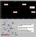
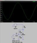
I want to design my own common emitter circuit. I don't know what points should be remember as an electronics engineer for this designing.
I have this knowledge:
1) I have input voltage 10mVpp
2) I want output 10Vpp
Is this sufficient knowledge for the designing of the CE circuit? (i.e. calculating the values of R1, R2, RC and RE and also Vcc and values of bypass capacitors and values of coupling capacitors.)
Thank you all.