Continue to Site

Welcome to EDAboard.com

Welcome to our site! EDAboard.com is an international Electronics Discussion Forum focused on EDA software, circuits, schematics, books, theory, papers, asic, pld, 8051, DSP, Network, RF, Analog Design, PCB, Service Manuals... and a whole lot more! To participate you need to register. Registration is free. Click here to register now.

[SOLVED] Low power colpitts oscillator trouble

Status
Not open for further replies.

Woody2

Newbie level 6
Joined
May 13, 2014
Messages
13
Helped
0
Reputation
0
Reaction score
1
Trophy points
1
Activity points
119
Hi,

I'm working on a project for school that includes this colpitts circuit from ALD.
https://www.aldinc.com/pdf/fet_11122.0.pdf

nlbipl.png


The main component being the zero-treshold mosfets (ALD110800).

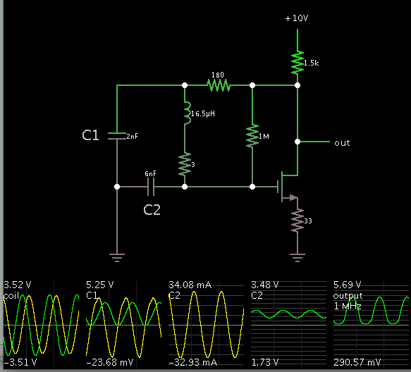
Now, the problem is that I can only use an inductor of 16.5µH, so according to the formula F=1/(2πvLC) I can lower the inductance if I raise the capacitance. So this is what I came up with for a colpitts running at 1MHz.

2u9gvap.png


However, I built this circuit but it seem to oscillate. So I ran some Pspice simulations. Things seem to be working fine here.

2vwi8ft.png

(Red being the drain of M1 and green being Vout.)

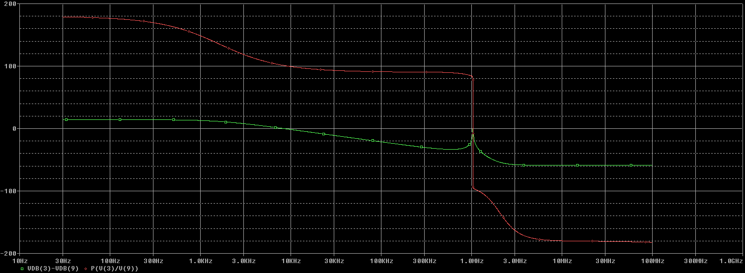
So I checked the phase shift to make sure I had a total of 360°.

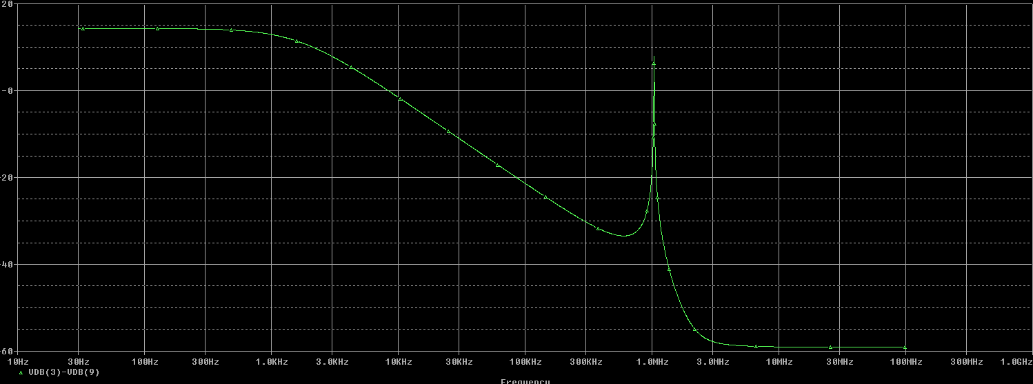
Here is the inverter
2n6uhc5.png

Shifting 171°, so the filter should be able to shift 189°
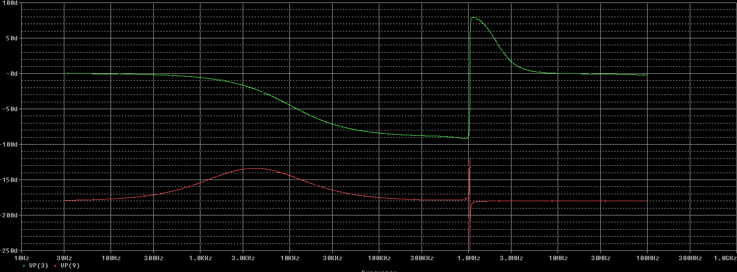
Here's the filter
9uy8e8.png

Not a problem.

Yet nothing happens in reality, what am I overlooking? :-?
Any advice is greatly appreciated.

ps:
In their schematic, ALD provides a capacitor in series with the inductor, yet information about this is nowhere to be found. In their simulations they didn't use it at all. We e-mailed them about this but never got a reply. Does anyone know the purpose is of this capacitor? Or what its value should be if used?

Thanks

When a third capacitor is added in series with the inductor, then it becomes a Clapp oscillator. Nevertheless this is still regarded as part of the Colpitts family.

As for what phase differences you expect in different parts of the circuit...
Remember when you read voltage across the coil or capacitor, it is 90 deg. out of phase with current going through it.
Additionally, the output may be distorted from a true sine shape. The mosfet may change state at a moment out of sync with another action which is aligned with a sine shape.
 

When a third capacitor is added in series with the inductor, then it becomes a Clapp oscillator.
No. A clapp oscillator has a completely different topology, non-inverting amplifier versus inveting amplifier with colpitts oscillator.

The only reasonable explanation is that C1 is intended as DC blocking capacitor with a relative high capacitance which doesn't affect the resonator frequency.

If you omit C1, Rf becomes useless and can be omitted too. The interesting question behind is, why is the gate bias provided by a high ohmic resistor instead of direct bias through L1? Gate leakage currents are said to be low, there's however a gate-source substrate diode present in the ALD MOSFET arrays, so the gate voltage will be shifted with sufficient high oscillation levels. I expect however that both circuit variants will work without large difference.

Apart from the confusion about C1, I don't understand what the original pots is exactly asking for. You don't show the simulation circuit, so we can only guess how the shown AC analysis has been achieved and what the phase value means.
 

Woody2 - regarding the ac analysis: You cannot expext correct results (loop phase 360 deg) if you simulate both parts (inverter and "filter") separately because they are not independent on each other.
Instead, for correct loop gain simulation you must open the loop at a suitable point and restore the load conditions and the bias point (if necessary).
However, in your case, a simpler procedure is possible because you have a high impedance node (gate): Place the ac source BETWEEN the gate node and the common node of RF and c1.
Then, the loop gain is the ratio of both ac voltages left and right to the ac source.
 
Last edited:

Thanks for the replies, I should have been more clear in the original post.
I'm making a bionic eye for school that uses this oscillator for inducance measurement, however, I can't get this circuit to work.
Colpitts testbord.jpg

I posted the simulations to try to show that this circuit should indeed work, but it doesn't and I dont know why.

I expect however that both circuit variants will work without large difference.

Tried them both (with multiple capacitor ratios/resistor values), they don't work. There's no oscillation but the DC values are as they should be.

Woody2 - regarding the ac analysis: You cannot expext correct results (loop phase 360 deg) if you simulate both parts (inverter and "filter") separately because the are not independent on each other.
Instead, for correct loop gain simulation you must open the loop at a suitable point and restore the load conditions and the bias point (if necessary).
However, in your case, a simpler procedure is possible because you have a high impedance node (gate): Place the ac source BETWEEN the gate node and the common node of RF and c1.
Then, the loop gain is the ratio of both ac voltages left and right to the ac source.

I see what you mean, I will try that now.
thanks
 
Last edited:

The 20k resistor at the supply wire restricts current to the circuit, and restricts oscillating action. A smaller value will help.

Below is my simulation, with some values altered.


Be aware a real mosfet may need greater bias voltage to turn it on. If C2 does not charge to sufficient voltage levels to do this, then you may need to substitute a transistor instead (as well as add components to provide suitable current bias).

A few mA is available at the output. The voltage swing may be wide enough, that a buffer stage is unnecessary.
 

Just changed the resistors to 1k,2.2k and 10k. No results :|. But you're right, it can't hurt to lower that resistor. I left the 10K. Lower values make the simulations go weird :smile:.
The mosfets are zero-treshold so bias voltage shouldn't be a problem.

Edit: what software did you use? Looks practical for this application.
 
Last edited:

The problem is simply one of Gate DC bias which lacks the gain in negative DC feedback due to C1 blocking DC.

You want the Vd avg. = V+/2 yet Vg threshold is fixed in this case appears to be near 2.5V but I am not familiar with the sub-threshold properties of this device suited for low voltage and zero voltage threshold.

Woody, in your plot, Vg starts at 3V and drifts down to 2.5 while Vd is too low and saturating, thus Vg is too high for these Zero bias FETs

Comparing the average Drain DC output with V+/2 is too low or saturated thus Vg is too high.

A simple test for a fixed V+ is a fixed R to Vgs to ground. such as 1~10M.

Consider this method recommended by AD.

Low-Voltage-Micropower-Lc-colpitts-Oscillator-Circuit-With-Active-Load.jpg
 

The problem is simply one of Gate DC bias which lacks the gain in negative DC feedback due to C1 blocking DC.

You want the Vd avg. = V+/2 yet Vg threshold is fixed in this case appears to be near 2.5V but I am not familiar with the sub-threshold properties of this device suited for low voltage and zero voltage threshold.

Woody, in your plot, Vg starts at 3V and drifts down to 2.5 while Vd is too low and saturating, thus Vg is too high for these Zero bias FETs

Comparing the average Drain DC output with V+/2 is too low or saturated thus Vg is too high.
A simple test for a fixed V+ is a fixed R to Vgs to ground. such as 1~10M.

Consider this method recommended by AD.
I think you misread the plot, it simply shows the drain of both mosfet's (inverter and buffer) to show the circuit oscillates. Alse we removed C1.
I made a Vg /Vd just now, your conclusion makes sense nonetheless.
We tried the active load circuit but got the same results.


Woody2 - regarding the ac analysis: You cannot expext correct results (loop phase 360 deg) if you simulate both parts (inverter and "filter") separately because they are not independent on each other.
Instead, for correct loop gain simulation you must open the loop at a suitable point and restore the load conditions and the bias point (if necessary).
However, in your case, a simpler procedure is possible because you have a high impedance node (gate): Place the ac source BETWEEN the gate node and the common node of RF and c1.
Then, the loop gain is the ratio of both ac voltages left and right to the ac source.

Assuming you ment Vg with left and Vd with right, here's the result:

Green =Vg red =Vd

The loop gain seems to be <1. I'm trying to figure out how to solve this.
Changing the capacitor ratio (bigger Cl1) seems to work wich seems very counterintuitive. however when Cl1>Cl2 weird things start to happen.

Guys thanks for the input, it amazes me how you guys can talk about this like its easy while me (and my teachers) sit here scratching our heads :roll:.

Code:
Colpitts oscillator
****************************
*    Colpitts Oscillator   *
*       with buffer        *
* Testing capacitor values *
*       Colpitss.cir       *
****************************


Vin	3	9	AC 0.1V

V+	1	0	DC 3.0V
VL	7	0	DC 3.0V

XM1	2	9	0 0 1 110800
*XM4	2	3	0 0 1 110800
*XM2	1	2	2 0 1 114804
R2 1 2 10k
XM3	6	2	0 0 1 110800

Rf		2	3	5.6E6	
Rout	6	7	2.7E3
Rl		2	5	60

Cl1	3	0	1.8E-9
Cl2	5	0	6.8E-9

L1	3	5	16.5E-6


.op
.OPTIONS ITL4=4000  ABSTOL=0.01 RELTOL=0.00001 
*GMIN = 0.1n
*VNTOL = 1M 
*.NODESET V(6)=1.17 V(2)=0.43 V(3)=0.43 V(5)=0.43 
*TRTOL=25 
*.OPTIONS ABSTOL = 0.01u  VNTOL = 10u  GMIN = 0.1n RELTOL = 0.05 ITL4 = 500 

*ABSTOL RELTOL
*.AC	DEC 1000 1k 20MEG

*--            d g s b v+
.subckt 110800 1 2 3 4 5 params: vtn=-0.037
m1 1 2 3 4 ncg l=7.8e-6 w=138e-6 as=0.603e-8 ps=0.478e-3 ad=0.161e-8
+                       nrd=0.3 nrs=1 nrg=25 nrb=35
.param vtx={vtn} cox=1.0 ires=0.41 pox=1.0 M=1
.model ncg  nmos  (level=1
+			 gamma=0.035 lot/4/uniform=-.22 dev/uniform=.04
+			 vto={vtn}   lot/2/uniform=.2   dev/uniform=19e-3
+             	 Uo=650      lot/3/uniform=40   dev/uniform=5
+             	 Ucrit=0.7e4 Uexp=.1 Vmax=1.6e5
+             	 phi=0.65 tpg=+1
+             	 nsub={1e16*ires} neff={10*ires} nss=0.7e11 nfs=4.4e11
+             	 tox=(0.055u*cox) lot/8/uniform=9.1% dev/uniform=.05%
+             	 Cgso={.94n*cox} Cgdo={.59n*cox} Cgbo={.138n*pox} Xqc=.42
+             	 cj=.39m cjsw=264p xj=1.0u
+			 ld=0.8u lot/uniform=.19 dev/uniform=.02 
+			 wd=1.05u lot/uniform=.42 dev/uniform=.1
+            	 pb=.9 js=20e-6  mj=.5 mjsw=0.18
+             	 kf=.75e-28 rsh=10 lot/1/uniform=4 dev/uniform=.5)
dbv 4 5 dps 0.8e-8
dbd 4 1 dps 0.8e-8
dbs 4 3 dps 0.8e-8
dbg 4 2 dps 0.8e-8
dgv 2 5 dps 0.8e-8
.model dps D (Is=2.61e-7
+             Isr=1.0e-5
+             Bv=34 Ibv=1e+4
+             Rs=2.74e-7 trs1=3e-3
+             Cjo=1.3e-4 )
.ends

*--------------d g s b v+
.subckt 114804 1 2 3 4 5 params: vtn=-0.4811
m1 1 2 3 4 ncg l=7.8e-6 w=138e-6 as=0.603e-8 ps=0.478e-3 ad=0.161e-8
+                       nrd=0.3 nrs=1 nrg=25 nrb=35
.param vtx={vtn} cox=1.0 ires=0.41 pox=1.0 M=1
.model ncg  nmos  (level=1
+			 gamma=0.035 lot/4/uniform=-.22 dev/uniform=.04
+			 vto={vtn}   lot/2/uniform=.2   dev/uniform=19e-3
+             	 Uo=650      lot/3/uniform=40   dev/uniform=5
+             	 Ucrit=0.7e4 Uexp=.1 Vmax=1.6e5
+             	 phi=0.65 tpg=+1
+             	 nsub={1e16*ires} neff={10*ires} nss=0.7e11 nfs=4.4e11
+             	 tox=(0.055u*cox) lot/8/uniform=9.1% dev/uniform=.05%
+             	 Cgso={.94n*cox} Cgdo={.59n*cox} Cgbo={.138n*pox} Xqc=.42
+             	 cj=.39m cjsw=264p xj=1.0u
+			 		 ld=0.8u lot/uniform=.19 dev/uniform=.02 
+			 		 wd=1.05u lot/uniform=.42 dev/uniform=.1
+            	 pb=.9 js=20e-6  mj=.5 mjsw=0.18
+             	 kf=.75e-28 rsh=10 lot/1/uniform=4 dev/uniform=.5)
dbv 4 5 dps 0.8e-8
dbd 4 1 dps 0.8e-8
dbs 4 3 dps 0.8e-8
dbg 4 2 dps 0.8e-8
dgv 2 5 dps 0.8e-8
.model dps D (Is=2.61e-7
+             Isr=1.0e-5
+             Bv=34 Ibv=1e+4
+             Rs=2.74e-7 trs1=3e-3
+             Cjo=1.3e-4 )
.ends

*Voor TRTOL
*.TRAN 10E-9 250E-6 0 1E-9 UIC

.TRAN 10E-9 500E-6 UIC

*.lib 11XXYY.lib
*.lib 11XXYY.slb
.PROBE
.END
 

Woody - I spoke about the AC analysis of the Loop gain function, which gives magnitude and phase vs. frequency (as requested by you).
Your display shows the results of a TRAN analysis.
 

Edit: what software did you use? Looks practical for this application.

The program is Falstad's animated interactive simulator. Free to download and use at www.falstad.com/circuit.

Or click the link below. It will:
(a) open Falstad's website
(b) load my schematic into his simulator, and
(c) run it on your computer.

**broken link removed**

You can observe current direction and intensity as they change through each cycle.

You can change values. Right-click on a component, and select Edit.

Saving and opening a circuit must be done via Import and Export, copying, pasting, using a word processor as the middleman.

Just changed the resistors to 1k,2.2k and 10k. No results :|. But you're right, it can't hurt to lower that resistor. I left the 10K. Lower values make the simulations go weird :smile:.
The mosfets are zero-treshold so bias voltage shouldn't be a problem.

It might work better to install a potentiometer and dial the correct DC bias voltage for the mosfet. (This sort of fine adjustment is often necessary to get an oscillator to the proper operating point.) A megohm pot is a suitable value which will not override the AC signal coming from LC tank.
 

Brad your link failed .. looks like a Falstad export scrambled with %20 spaces in the link

Also I doubt Falstad has the library file for the Zero threshold MOSFET.

But it is a great simulator for basic functions, like Bode plots and timing diagrams of small scale analog and digital.
 

Brad your link failed .. looks like a Falstad export scrambled with %20 spaces in the link

Also I doubt Falstad has the library file for the Zero threshold MOSFET.

But it is a great simulator for basic functions, like Bode plots and timing diagrams of small scale analog and digital.

Yes, tinyurl.com provided a corrupted link.
Now that I tried again here is this one which works:

https://tinyurl.com/mferl7o

From my experience, the mosfet model in Falstad's simulator does not turn on fully unless it is biased abnormally high. There is only a parameter setting for 'threshold voltage'. It seems to have only slight effect on overall operation of the mosfet.
 

Did I miss something or is it true that you gave no clear problem description at all?

If I understand right, the problem is that the real circuit doesn't oscillate, so it's most likely not a simulator problem. I have no doubt that the original circuit can oscillate with the original parameters. If your circuit is not working, you should primarly look for the differences.

Obviously you reduced the LC circuit (if the assumed L value is correct) impedance √(L/C) by a factor of about 3. This can be sufficient to prevent oscillation at low drain currents and respective low gm. You should better scale L and C with the same factor, keeping the original Z. In addition, are you sure about the real coil inductance? I only see a small air coil in the circuit photo.

The problem is that the real circuit doesnt oscillate. So we went to simulations to find out why.
In simulations everything seems to be working fine however so we're left to wonder why it doesn't work in reality.
We've tried about everything, including decreasing C to a smaller value keeping the original impedance conditions like you said.

The inductor was calculated and measured, its definitely 16.5µH (5 layers of very thin wire!)

I'm studying up about loop gain and came up with this graph AC analysis:

The loop gain seems fine to me at 8/1MHz

I don't know however how to interpret this phase graph though

I'm discussing this with my teacher tomorrow, keep in mind I'm pretty new at this.

Thanks guys, the falstad software will make for some cool pictures in the powerpoint :grin:
 
Last edited:

I'm studying up about loop gain and came up with this graph AC analysis:

The loop gain seems fine to me at 8/1MHz

I don't know however how to interpret this phase graph though

* I suppose, you know that the loop gain must cross the 0 dB line at the desired frequency?
* Yes - the interpretation of YOUR graph is not so simple because you have two curves) .
However, why not plotting the P(V(x)/V(y)) ?
 

The discussion about the correct way of loop gain simulation is surely of general interest. Understanding how circuit parameter variations influence the loop gain and fulfillment of oscillation conditions can be also helpful to debug the real circuit.

To check the operation of the real circuit, it would be however preferable to validate the amplifier and LC circuit operation in hardware. If you have a function generator and an oscilloscope, you can "see" the loop gain in the real circuit.
 

* I suppose, you know that the loop gain must cross the 0 dB line at the desired frequency?
* Yes - the interpretation of YOUR graph is not so simple because you have two curves) .
However, why not plotting the P(V(x)/V(y)) ?

Ok I get it now.

Makes alot more sense :smile:

The discussion about the correct way of loop gain simulation is surely of general interest. Understanding how circuit parameter variations influence the loop gain and fulfillment of oscillation conditions can be also helpful to debug the real circuit.

To check the operation of the real circuit, it would be however preferable to validate the amplifier and LC circuit operation in hardware. If you have a function generator and an oscilloscope, you can "see" the loop gain in the real circuit.

You're right, we tried this before but I think we were doing it wrong, we were just injecting the AC signal.
Instead I suppose we have to open the circuit at the gate and measure the way LvW suggested earlier:

However, in your case, a simpler procedure is possible because you have a high impedance node (gate): Place the ac source BETWEEN the gate node and the common node of RF and c1.
Then, the loop gain is the ratio of both ac voltages left and right to the ac source.

Working on this right now
 

Ok I get it now.

Makes alot more sense :smile:

To me, it does not make sense. For an oscillator, I expect that the loop phase at the gain crossing point (0 dB) also is zero (360 deg).
Something is still wrong in your circit.
 

To me, it does not make sense. For an oscillator, I expect that the loop phase at the gain crossing point (0 dB) also is zero (360 deg).

It roughly is, I think, although you can't clearly see if the gain is above or below 0 dB. According to the time domain waveform, it is above unity. The high resonator Q however belongs to the world of unrealistic simulation circuit assumptions. Seeing a gain of -20 dB or -30 dB at frequencies near resonance gives an idea what probably happens in a real circuit with lower Q.

I must also report a calculation error in my post #9 as I said, the resonator impedance would differ between the original circuit and the 1 MHz variant by a factor of 3. But it's actually factor 100, 10 k reduced to about 100 ohm.
 

Status
Not open for further replies.

Similar threads

Part and Inventory Search

Welcome to EDABoard.com

Sponsor

Back
Top