Continue to Site

Welcome to EDAboard.com

Welcome to our site! EDAboard.com is an international Electronics Discussion Forum focused on EDA software, circuits, schematics, books, theory, papers, asic, pld, 8051, DSP, Network, RF, Analog Design, PCB, Service Manuals... and a whole lot more! To participate you need to register. Registration is free. Click here to register now.

FEM analysis for CPW line in ADS 2011

Status
Not open for further replies.

harsimran315@gmail.com

Newbie level 5
Joined
Feb 18, 2014
Messages
9
Helped
0
Reputation
0
Reaction score
0
Trophy points
1
Activity points
56
Respected all
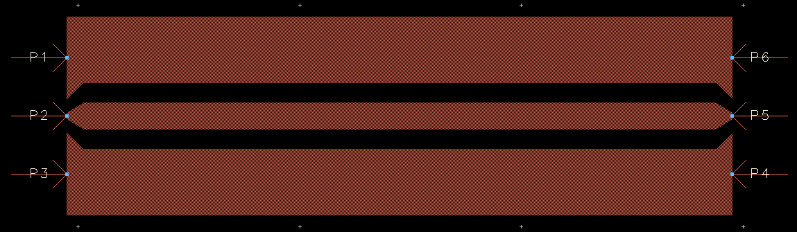
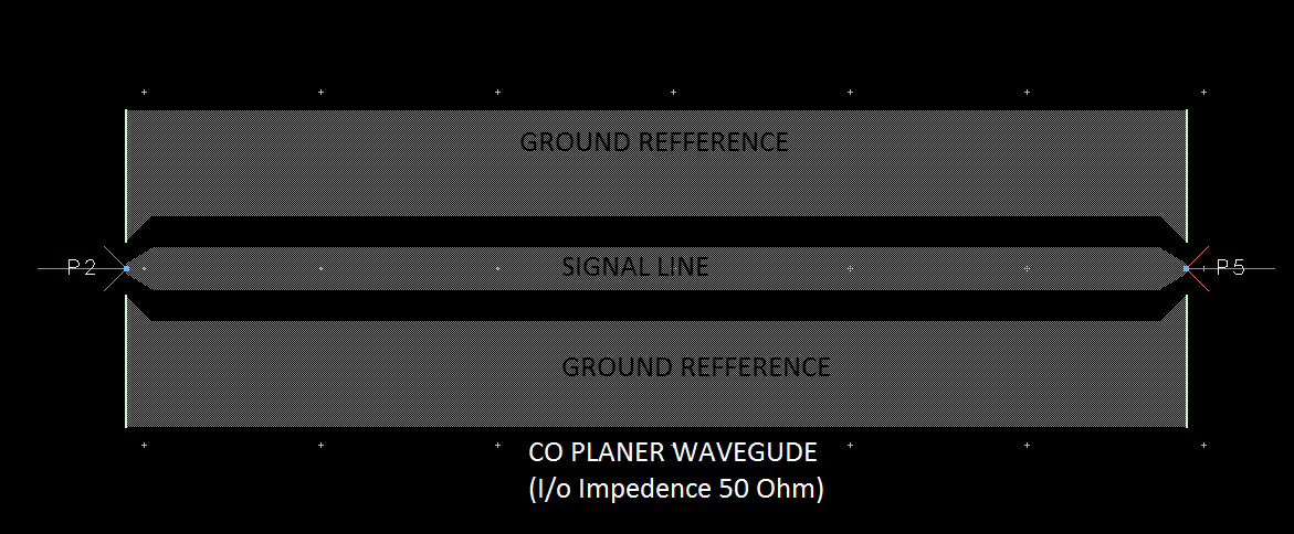
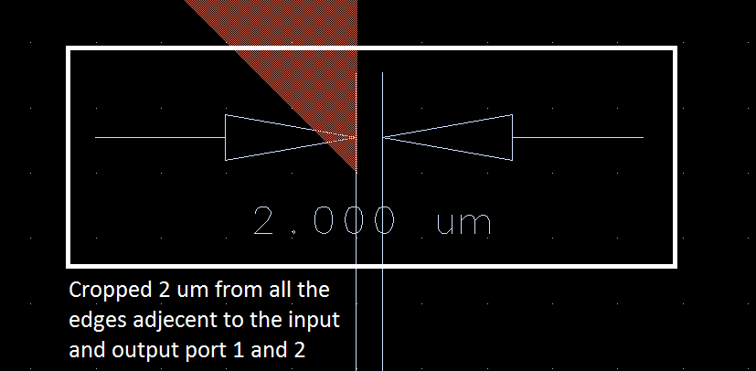
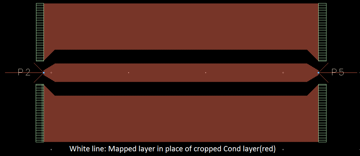
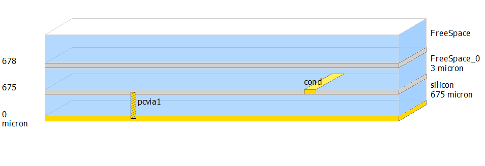
can anybody help me out that how to apply ports in ADS 2011 for FEM analysis of a CPW line. The previous version used a different method of making ports as ground reference but ADS2011 does not have the facility to do so.
 

Respected sir
I tried this method. Please refer to the image shown. I want the central line to be signal and side lines to be ground reference. and i tried to implement the method of slot lines but when i start the FEM analysis it says that magnetic ports are not valid.
PS port 1,2 are input and output (+ve)
and port 3,4,5,6 are (-ve).
As i want the layer connected to be ground refference
 

Instead of stripline definition for your metal in your substrate definition, use slotline.

That is for Momentum only, not for the FEM solver.

- - - Updated - - -

in ADS 2011 for FEM analysis of a CPW line.

Why do you want to use FEM, and not Momentum? Momentum is more efficient for this type of models, especially if you use the "slot meshing" method that johnjoe mentioned, where the slot is meshed instead of the metal.

The previous version used a different method of making ports as ground reference but ADS2011 does not have the facility to do so.

For your existing setup:
In the port editor, use drag & drop to move P1 and P3 to the (-) terminal of P2. This creates a differential port where P1 and P3 are the negative terminals for P2.
 
That is for Momentum only, not for the FEM solver.

- - - Updated - - -


Why do you want to use FEM, and not Momentum? Momentum is more efficient for this type of models, especially if you use the "slot meshing" method that johnjoe mentioned, where the slot is meshed instead of the metal.

I want to do a comparitive analysis of both the solvers


For your existing setup:
In the port editor, use drag & drop to move P1 and P3 to the (-) terminal of P2. This creates a differential port where P1 and P3 are the negative terminals for P2.

the method you told is valid for Momentum but not for FEM which is my problem. Rest what you told is the same procedure that i follow
 

Sir
can you please specify the method for solving the circuit (FEM)
i am just confused about the port connection so that the extreme side conductor is ground plane and central conductor is signal line
 

If you really just want to simulate the structure shown, take MoM, its results are reliable. Otherwise, please explain why you're "forced" to use FEM.
 
the method you told is valid for Momentum but not for FEM which is my problem. Rest what you told is the same procedure that i follow

Sorry, you are right. FEM does not support multiple (-) terminals. Use Momentum instead.
 
Maybe on hint, as I remember you can use a box (PEC) to enclosure your design. If both ground planes touch the sidewalls of the box and you can somehow set your port correctly, maybe it works. But I can't check it for you and consider the manual for the use of the box. But maybe I'm wrong. The next problem is that the box, and thus your ground planes, has to be large enough to not interfere with your structure. But this would result in large EM-Problem. Depending on your computer capability, I suggest to take MoM, like Volker and me said before.
 
To all those expecting a solution to the above problem.
i worked hours on it and trying to do the above said and finally found the solution
A simple way to make the ground line of CPW, MEMS switch or any planer device and run FEM is by doing as follow.
before that pls reffer to the figure (Figure 1)


1. Crop the ground substrate by say 2-3 um from the ends (Figure 2)


2. Map a layer in place of cropped area (Figure 3)


3. Ports are connected to signal line.

4 create Substrate defination and via the newly mapped layer to the ground (Figure 4)


In this way the plane connects to ground and acts as a ground reference

A comparitive analysis of MOM and FEM was done and their same characteristics proves the validity of the same
 

Mhmm, ok but you wrote you want to simulate a cpw structure, not a gcpw. These are two different structures! Because a gcpw is easier to simulate, as you did.
 
And btw, you see there is almost no big difference between MoM and FEM for your application ;-).

Yes sir the results are almost same as i have just simulated a simple CPW line but the results will tremendously vary when ill make a SPST MEMS shunt capactive switch or a series ohmic switch.
CPW line being planer shows no variations ,But a switch being a non planer device will show variations
 

Mhmm, ok but you wrote you want to simulate a cpw structure, not a gcpw. These are two different structures! Because a gcpw is easier to simulate, as you did.

I agree.

Instead of simulating an ungrounded CPW with ground below the substrate, the better approach would be to draw some bridge metal (which also exists in real CPW hardware at bends/junctions) on a layer that is closer to the CPW metal.

The difficulty with the ground on the bottom of the substrate is the via length, and the mode excitation. The single ended ports create an excitation to the infinite ground below the substrate, and the CPW grounds are then connected to the infinite ground through the vias (with some path length = inductance). This isn't exactly what we have in hardware/measurement.

- - - Updated - - -

when ill make a SPST MEMS shunt capactive switch or a series ohmic switch.

Ok, in that case FEM can be useful. But from my own experience with MEMS EM simulation: you should be careful with the GCPW port configuration that you have shown - it isn't correct. You should not simulate backside grounded GCPW if your hardware is CPW.
 

Status
Not open for further replies.

Similar threads

Part and Inventory Search

Welcome to EDABoard.com

Sponsor

Back
Top