Continue to Site

Welcome to EDAboard.com

Welcome to our site! EDAboard.com is an international Electronics Discussion Forum focused on EDA software, circuits, schematics, books, theory, papers, asic, pld, 8051, DSP, Network, RF, Analog Design, PCB, Service Manuals... and a whole lot more! To participate you need to register. Registration is free. Click here to register now.

Is the device capacitance bias-dependent or independent?

Status
Not open for further replies.

Alex Liao

Member level 4
Joined
Apr 8, 2013
Messages
75
Helped
2
Reputation
4
Reaction score
2
Trophy points
1,288
Activity points
1,991
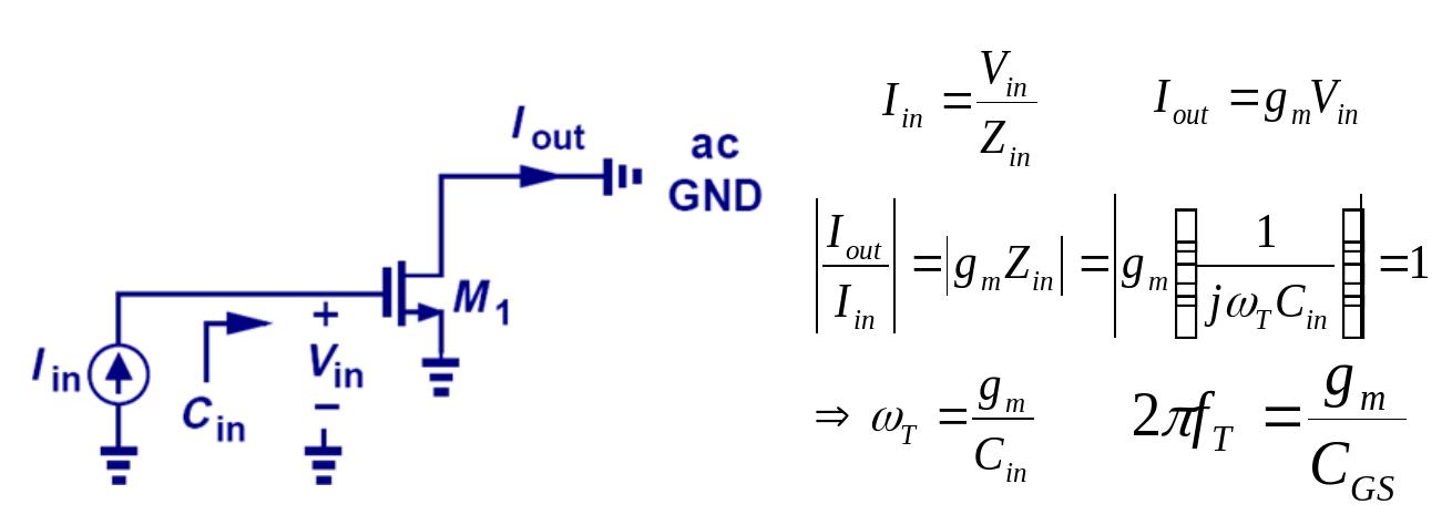
Hi, I would like to know if the device intrinsic capacitance like Cgs bias-dependent or independent. Giving say, bias 400mV or 500mV (common source circuit with Vgs = 400mV or 500mV) for 65nm technology, is the Cgs the same or different and why?

Thanks,
Alex
 

Yes the Cgs capacitance is voltage dependent capacitance.
Hope the following references will help:

1) Chapter 2, Section 2.4.2 Mos Device Capacitance Page No: 29 from the book **broken link removed**

2) The Voltage-dependent capacitors section from http://en.wikipedia.org/wiki/Capacitance

3) **broken link removed**

Hope it will help ... :)
 
Thanks a lot!:cool:

By the way, in your third source, in Unity Gain frequency fT of MOS transistor part, do you know what does the (s) in Id(s) and 1/s in Vgs(s) mean?

- - - Updated - - -

Thanks a lot!:cool:

By the way, in your third source, in Unity Gain frequency fT of MOS transistor part, do you know what does the (s) in Id(s) and 1/s in Vgs(s) mean?

Is s = 2 * pi * f?
 
Last edited:

Anything with a depletion region on either side of it will be
voltage dependent. MOS channels swing from accumulation
through depletion to inversion. Cgs follows gate voltage
directly; Cgd, only when the channel is well lit near the drain
(linear region - when it goes constant current the capacitance
is sort of stood off from the channel by the pinch. The
partitioning with drain voltage is a messy thing to get right.

The overlap capacitances are less voltage dependent, if
you do not have poly depletion anyway. Mostly fringing
fields through the various oxides. You can't meaningfully
deplete a >1E20 doped S/D region even if it wasn't silicided.
 
Hi Alex Liao

Thanks a lot!:cool:

By the way, in your third source, in Unity Gain frequency fT of MOS transistor part, do you know what does the (s) in Id(s) and 1/s in Vgs(s) mean?

Agreeing with , Dominik Przyborowski, the s is the complex variable in Laplace domain. They are calculating the transfer function Id/Ig in Laplace domain for calculation of Transit frequency ft.
The “transit” or “cut-off” frequency, fT, is a measure of the intrinsic speed of a transistor, and is defined as the frequency where the current gain falls to 1.

Hope the picture explains:

 
Thank you (SIDDHARTHA HAZRA, dick_freebird and Dominik Przyborowski) so much!
 

Status
Not open for further replies.

Part and Inventory Search

Welcome to EDABoard.com

Sponsor

Back
Top