Continue to Site

Welcome to EDAboard.com

Welcome to our site! EDAboard.com is an international Electronics Discussion Forum focused on EDA software, circuits, schematics, books, theory, papers, asic, pld, 8051, DSP, Network, RF, Analog Design, PCB, Service Manuals... and a whole lot more! To participate you need to register. Registration is free. Click here to register now.

LDO with current FB amplifier

Status
Not open for further replies.

kingearlkwan

Junior Member level 1
Joined
Apr 26, 2013
Messages
15
Helped
0
Reputation
0
Reaction score
0
Trophy points
1,281
Activity points
1,393
Hi Guys,

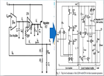
Need some help understanding the circuit attached. The circuit utilizes an OTA error amplifier with current fb amp to improved transient response. Can anyone help me explain in details how the ckt behaves specially on the transistor levels when it encounters a current load variations?

Thanks!
 

Attachments

  • Untitled.png
    Untitled.png
    127.2 KB · Views: 93

I am surprised that the unit that is driven by the OTA is called "CFA".
Normally, a CFA has a low-resistive voltage output.
An integrated unit with a high-resistive non-inv. input, a low-resistive inverting input and a high-resistive current output (as shown in the picture) is classifies as a current conveyor type II (CCII).

Independent on this classification:
Together with the FET this "CFA" (more correct: CC) forms a composite amplifier that has a non-inverting characteristic (related to the high-resistive CC-input).
Hence, for overall negative feedback an additional signal inversion is necessary.
This requires an additional amplifier (OTA) because the inverting low-resistive CC-input cannot be used for this purpose.
I suppose, at this place an OTA is used (instead of a classical voltage opamp) because its simplicity.
 
Last edited:

Hi LVW,

Thanks for your reply.It seems that it has a lot of prerequisite ideas that I need to learn.Is it okay if you can explain more in details your point? Can we take an example like if there is an increase in current load, how does the ckt works to regulate the output?I understand that the used of CFA on this ckt is for fast slew rate during load variations,but i'm still confused on how the ckts works. Also, Why used folded cascode instead of the ordinary voltage error amp?What is the advantage of folded cascode? Am I correct that the purpose of the current mirrors on the OTA side serves only as active load to provide higher output impedance which lead to higher gain?Pardon me for asking too much, I just need to understand it better. I know I can research on some simple questions that I've asked but sometimes explanations on books and other materials needs a higher level of comprehension and solid foundations on this for a newbie like me. Thanks!

- - - Updated - - -

Btw, you mean that the 2nd stage FB is a CC type two and not a CFA?what's the difference between the two? I only read this ckt in one of the IEEE paper and the author called it as CFA.I'm not sure of the difference between CFA and CC. Thanks for your feedback!
 

At first, let me say that it is always a bit "problematic" to explain in detail the working principle (and the dimensioning) of a circuit designed by somebody else.
Nevertheless, here are some explanations:
The LDO consists of two parts: A regulated amplifier Ar (FET & CFA) and a control loop (error amplifier Ae).

* The amplifier Ar is composed of a FET in common source configuration with negative feedback. This feedback loop consists of a current conveyor (CCII-) with an additional load impedance. This combination can be regarded as a CFA with a pretty high output impedance.
* The control loop contains an OTA (also with a load impedance) which regulates the amplifier Ar via negative feedback.

* In summary:
We have a system with a "small" internal local loop (FET & CFA) and a "large" outer loop (Ar & OTA). It is a common method for control systems to use such a double-loop system, because the inner loop is quicker and can react with less delay upon changes.
This can also be explained as follows: Local negative feedback increases the bandwidth of the FET amplifier, thus allowing a step response with a smaller time delay (delay is always invers proportional to bandwidth).

Note on CC: High resistive Input Y , low-resistive input X, high-resistive output Z.
Two types are possible:
CCII+ : Ix and Iz both flowing into the terminal or out of the terminal (Ix=Iz)
CCII- : Ix=-Iz (as indicated by the current directions in the diagram, we have a CCII- type).
Comment: The currents of the CCII- type can be compared with BJT transistor currents Iy~Ib, Ix~Ie and Iz~Ic. Therefore, the CCII- sometimes is called "ideal" transistor or "diamond transistor".

I hope , the above explanations can help to understand the working principle of the circuit.
 
Last edited:

Status
Not open for further replies.

Part and Inventory Search

Welcome to EDABoard.com

Sponsor

Back
Top