kabaleevisu
Advanced Member level 2
- Joined
- Apr 14, 2010
- Messages
- 616
- Helped
- 85
- Reputation
- 170
- Reaction score
- 81
- Trophy points
- 1,308
- Location
- Chennai,India
- Activity points
- 4,512
Hi everyone,
right now i am migrated into altium designer.i did small schematic and import in altium layout.let me know follow detail from altium designer.
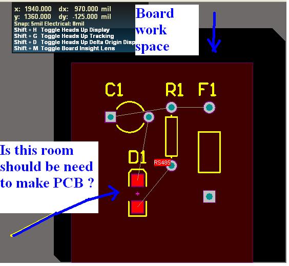
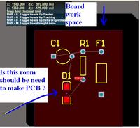
1.while import components are assign as room property is it need ??if multiple of sheet is available that time what i have to do is i need to keep in board workspace ??
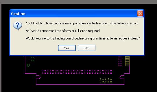
2.how to make the origin for board outline ??
3.how to assign the origin while importing DXF in altium ?
please reply any one for this queries .......
right now i am migrated into altium designer.i did small schematic and import in altium layout.let me know follow detail from altium designer.
1.while import components are assign as room property is it need ??if multiple of sheet is available that time what i have to do is i need to keep in board workspace ??
2.how to make the origin for board outline ??
3.how to assign the origin while importing DXF in altium ?
please reply any one for this queries .......