Continue to Site

Welcome to EDAboard.com

Welcome to our site! EDAboard.com is an international Electronics Discussion Forum focused on EDA software, circuits, schematics, books, theory, papers, asic, pld, 8051, DSP, Network, RF, Analog Design, PCB, Service Manuals... and a whole lot more! To participate you need to register. Registration is free. Click here to register now.

Calculating transmission and reflection coefficients of a multilayered structure

Status
Not open for further replies.

Mona7150

Member level 1
Joined
Nov 9, 2013
Messages
35
Helped
0
Reputation
0
Reaction score
0
Trophy points
6
Activity points
249
Hello all,

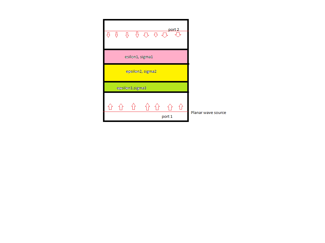
I have to determine S11 and S21 for a planar multilayered structure ( different layers with different permitivities stacked on each other). The thickness of different layers is fixed only in one dimension(say Z-axis,total thickness in Z direction is almost 150mm). My frequency of operation is around 403MHz. I tried doing it with CST and HFSS but since they are 3D software so I am not able to understand what thickness should be kept in the other two axis(x and y axis) because the results change as I change these dimensions. Moreover do I need to make some changes in mesh settings?
Can anybody please suggest some other way of solving the problem?


Thank You
 

Can you make a drawing of your structure including excitations (ports or plane wave), just to avoid miscommunication?
 

The picture is vague in several regards.
- what are the horizontal boundaries?
- what's the nature of the ports? There must be some kind of coupler at both ends.

This doesn't look like what we know as a planar wave guide, neither the said "planar wave source" corresponds to known topologies.
 

The picture is vague in several regards.
- what are the horizontal boundaries?
- what's the nature of the ports? There must be some kind of coupler at both ends.

This doesn't look like what we know as a planar wave guide, neither the said "planar wave source" corresponds to known topologies.

Sorry for the incomplete information. This is actually a biological tissue I am trying to simulate. For example the three layers are the muscle,fat and skin layers of a human tissue. My aim is to determine the equivalent S11 and S21 for the whole structure. Please refer to the new attached image where d1,d2 and d3 are the biological thicknesses of these layers. By plane wave source I mean a source giving out plane waves. In CST I have tried using waveguide ports. Rest of the details are mentioned in my first post in this thread.

I don't know whether I have been able to put my problem clearly. Please let me know.

https://obrazki.elektroda.pl/8010800200_1391951854.png

Thanks
 

When I understand you well, you have plane wave excitation arriving at theta = 0 (so the waves arrive from positive Z direction). Your dielectric layers are in the XY plane. You want to know S11 and S21 for the plane waves.

If you use plane wave excitation and want to know what happens because of the dielectric only (so excluding diffraction effects), you need to use infinite dielectric size in the XY plane. Such problems can be solved with a MoM simulator with short runtimes.

You should base your meshing (when required to enter manually) on the smallest wavelength. Assuming that 2*pi*f*epsr*eps0 >> conductivity, the wavelength depends on epsr only. You may know c = c0/rt(epsr). epsr = relative dielectric permittivity.

Very likely your simulator has accuracy settings. Check the documentation on how to use these settings.

For simulators that can't handle infinite dielectrics efficiently, it is more elaborate. You need to increase the size of the dielectrics so that the dielectrics cover about the first 2 or 3 fresnel zones as seen from the observation piont where you determine E an H. In addtion the dielectrics should be very large w.r.t. free space wavelength to avoid internal resonances (similar to MIE scattering around a sphere).

When everything is fine, gradually increasing the size of the dielectric layers, should result in variation of measuring results within your required accuracy.


I see that you are using organic tissue. In that case you need to determine the propagation constant based on complex permittivity or complex conductivity. From the propagation constant you can determine the wavelength in the dielectric. In very lossy dielectrics the wavelength depends on Re(conductivity) or Im(permittivity) also.
 
Plane wave makes sense (in contrast to "planar" wave). It's of course a simplification of a real wave transmission problem, but you should be able to derive reflection and transmission coefficients.

The 3D EM problem reduces to a one-dimensional transmission problem with perpendicular boundary layers, similar to reflection and transmission in optical multilayers.

I'm not so familar with these EM simulators and can't tell you how to setup a plane wave problem. But actually you don't need a 3D EM-solver to calculate it.
 
  • Like
Reactions: WimRFP

    WimRFP

    Points: 2
    Helpful Answer Positive Rating
Thank you for the reply Sir.
Yes, you understood the problem well. Actually I have tried the problem in IE3D which is based on MOM, but in IE3D with each dielectric layer there is some sort of metallic layer associated which can't be deleted. So I thought this might not help me to solve the problem. Can you please suggest some other MOM based simulator?

Moreover till now I don't know whether HFSS(FEM based) and CST (FDTD based) can handle infinite dielectrics. I will try to ponder over all the points you made and then get back to you.

Thanks

- - - Updated - - -

@ FvM

Sir, if it can be solved otherwise ,can you please suggest some book or paper which can help me solving the problem ?

Thanks
 

Regarding IE3D:
You can do it with IE3D. There is no metallic layer between the dielectrics, unless you specify them. you can specify dielectric layers indepent from metallic layers in IE3D.

The zero heigth layer is metallic by default, but when you go to the basic parameters window, you can set the conductivity to zero, and then there is no metallic layer (only air down to Z= -infinity). Note that you can only specify structures above Z=0, so if you want some metallic structure below your stack of dielectrics, you need to raise your stack so that you have heigth above Z=0 to draw your structure.
 

@ WimRFP

In IE3D, in "basic parameters" window I define all my dielectric layers in "substrate layers" option and set the conductivity of ground plane zero. But just adjacent to "substrate layers" option is "metallic strip types" option in which some isotropic/non isotropic metallalic types are defined. This can't be deleted so I made its conductivity= 0 but once simulation is started it gives me following error..."No.1 Metallic Strip: Incorrect parameters(ic=-6 type=0)" . I am unable to remove this error.
 

The z=0 layer should only have zero conductivity (that means you need to change one parameter only). When done, there will be no dashed line in the color representing the Z=0 layer. It is best that you don't change other metallic layers.

You can draw metallic structures on other layers, but when you draw nothing, there will be no metal at the interface between different dielectric layers. The program shows metallic layers at interfaces as normally there will be metal (as in a multy layer PCB), but it will only be there when you actually draw polygons.

- - - Updated - - -

By default, the dielectric layers in IE3D are infinite in x and y direction. In newer version you can convert a polygon into a finite size dielectric layer. The version of IE3D I have access to can only handle infinite dielectric layers and uses the old data format (not html like).

- - - Updated - - -

How you are going to "measure" the incident field, reflected field and transmitted field? I used short electric dipoles. I "calibrated" the dipoles by first simulating plane wave excitation in free space and compared this with theoretical expectation.
 
Hi, Have you solved the problem? If you are interested, i can try to explain my experience in CST about modelling of multilayer structure as carbon fiber.
 

Thank you zionico90.
No I haven't solved it yet. It will be great if you can help me out.

- - - Updated - - -

@wim

Can I please send you my design that I have implemented in IE3D so that you can check it?
After defining the layers, I have used rectangles to draw the actual structure using polygon editor. I have randomly taken 100 x 100 dimension for the rectangles but as pointed out by you the dielectric should be infinite in x and y directions. Can IE3D handle infinite dielectrics and how ?

Thanks
 

Do you have more informantions about the materials?

- anisotropic or isotropic materials?
- thickness?
 

Do you have more informantions about the materials?

- anisotropic or isotropic materials?
- thickness?

Yes. I am assuming the materials to be isotropic and thickness is also defined as mentioned in my previous post.
 

Sorry, but I don't find the thickness of d1,d2 and d3. In any case, if the thickenss are less than 1mm, it is necessary to create a normale material and an associate thin panel material. For thickness less than 1 mm, CST guarantees good accuracy only if thin panels are used. Finally, considering a unit cell of multilayer material and using "period" as boundary condition (and open in the propagation direction) with a plane wave it is possibile to find the s-parameters in order to caraterize the structure.
 

@Zionica90
Sorry I didn't mentioned the dimensions in the figure. Well, the least thickness I have is 3mm. Others being 10,20,90,10 mm making a total thickness of the layered structure around 150mm. But I don't know how to make the other two dimensions as infinite( approx what value means infinite). I am using a waveguide port, "normal" as background material, "open" boundary conditions, "none" symmetry plane, "open " for thermal boundaries( not sure about it),units in 'mm' and frequency in "MHz". Just to check the design I used a simple box with only vacuum and above specifications but it gives me 0.99 as the value for S11.
What do you mean by "period" in boundary condition?

Thanks

@wim
After making the design in IE3D and assigning ports I directly simulate the structure to give s-parameters.I can't understand that why do I need to measure electric fields separately . Please see the attached image. This has been done for 100 x 100 mm rectangle. The main problem here was that I presumed there is a metallic layer which gets associated with each dielectric layer as mentioned before . As you mentioned before, metallic layer will be there when we draw polygons, so shouldn't it be there in my case also?

https://obrazki.elektroda.pl/7293523900_1392270906.png
 

I don't recognize the structures with 1 and 2 in it (it seems you have a new version if IE3D). Are these plane wave ports? If so you don't need to use dipoles to measure the plane wave field properties.

Try you setup with something you can calculate by hand (for example a quarter wave and a half wave thick lossless dielectric).

If this works well, you don't need to draw any metal. When required, you can draw metallic structures everywhere (that means inside dielectric not being bounderies, or just somewhere in air).


I don't understand why you need the 100*100 structure.
 

@ wim

Yes, these are the plane wave ports defined in air medium. 100x100 is just an example dimension I had taken because I didn't knew that they should be infinite in my case. I will try to simulate a quarter wave dielectric.

Is it that after defining substrate layers( without changing anything in "metallic types" tab) and then drawing infinite ploygon , the metallic layer which is by default there in "metallic types" won't get associated with my dielectric layers?
 

IE3D creates layers for drawing metallic structures at each dielectric layer you define. So when you add another dielectric layer, you get a new metallic layer (but there is no metal, only when you build polygons you get metal). In addition to this, you can add other metallic layers at any height. Only the Z=0 layer is default present as an infinite ground plane, but setting conductivity = 0 for the Z=0 layer removes the ground plane.

You may know that newer version of IE3D do support finite size dielectrics.

I don't understand your point regarding "drawing infinite polygons".

"metallic types" option does not change the dielectrics. By defining metalllic types you can assign a number to polygons, so IE3D enables you to use material with different conductivity and thickness within one structure.
 

Status
Not open for further replies.

Part and Inventory Search

Welcome to EDABoard.com

Sponsor

Back
Top