Continue to Site

Welcome to EDAboard.com

Welcome to our site! EDAboard.com is an international Electronics Discussion Forum focused on EDA software, circuits, schematics, books, theory, papers, asic, pld, 8051, DSP, Network, RF, Analog Design, PCB, Service Manuals... and a whole lot more! To participate you need to register. Registration is free. Click here to register now.

[SOLVED] Accuracy of Leakage models in TSMC 180nm

Status
Not open for further replies.

nitishn5

Full Member level 6
Joined
Mar 27, 2011
Messages
365
Helped
91
Reputation
184
Reaction score
98
Trophy points
1,308
Location
Bangalore, India, India
Activity points
4,129
How accurate is the leakage models of both core and high voltage devices in the TSMC 180nm process?

In my simulations, the numbers are very small and of the order of 10s of femto-amps on a node with just two small drains connected to it.
But silicon shows an extra current in the order of 100s of pico-amps unaccounted for.

I was not expecting the leakage current of some small devices to become so large.
This shows an increase by at least 3 orders of magnitude.

Are the models that bad for such a mature process? Or are these numbers so small that this is the best accuracy that can be achieved?
 

In my experience the "leakage" modeling always gets
hind teat when it comes to priorities, especially in a
"digital" flow.

Your current seems large and I hope you have at least
tried to do a probes-up I-V to de-embed any harness
and instrument leakage floor. And remembered to leave
the lights off, because exposed chips can have a lot
of photocurrent (relatively speaking) under ambient,
let alone micrscope illuminator, light input. A black tent
is a good idea. It's also possible that, on wafer, you
do not have full control of all device nodes, or that
the chuck has too much 60Hz hum on it and you're
rectifying that through the isolation junctions and
collecting the "bonus" current.

Leakage might be diode conduction or might be MOS
subthreshold conduction, DIBL / GIDL, etc. Some of
these are not well fittable by older models, and some
are subject to process variation and might only be
well represented at corner model conditions, if you
happen to have off-center material in hand.

That low voltage technology is also liable to not be
very resistant to handling overstress and you could
be inducing abnormal leakage by your test equipment
simply touching down while precharged, or walking in /
walking out leakage by repeatedly sweeping past or
through hot-carrier-inducing regions of operation.
 

Thanks dick_freebird,

The chip is complete with packaging. The node in question is within the chip and has no access to the outside. It has only a couple of devices connected to it which have sufficient negative Vgs to turn them off. The only other thing it sees are gates. So external influence is not of much concern.

The numbers being off by a few orders of magnitude is what surprised me.
 

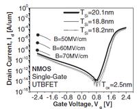
If "sufficient negative Vgs" is significantly below zero,
GIDL phenomena will raise the leakage floor above what
a typical WAT test condition would show. Digital flows
will optimize for a leakage null near, but slightly below
(for capability statistics) Vgs=0; going more negative
does not improve leakage.


Status
Not open for further replies.

Part and Inventory Search

Welcome to EDABoard.com

Sponsor

Back
Top