Continue to Site

Welcome to EDAboard.com

Welcome to our site! EDAboard.com is an international Electronics Discussion Forum focused on EDA software, circuits, schematics, books, theory, papers, asic, pld, 8051, DSP, Network, RF, Analog Design, PCB, Service Manuals... and a whole lot more! To participate you need to register. Registration is free. Click here to register now.

SPWM Inverter - IR2110 and IGBT high side problem

Status
Not open for further replies.

martin_t

Newbie level 6
Joined
Dec 23, 2013
Messages
11
Helped
0
Reputation
0
Reaction score
0
Trophy points
1
Location
Buenos Aires, Argentina
Activity points
113
Hello guys.
This is my first post here, though I've been going trough the forum for rather some time.
I´m designing an inverter based around a dsPIC33FJ128MC802 and two IR2110 in a full bridge configuration driving four IRGP4063D IGBTs.
The PWM signal is switching at 20khz and the DC Bus voltage is 40Vdc, and the AC output is 220 Vac 50hz through a step up transformer and capacitor in parallel.
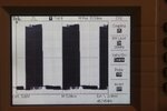
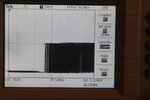
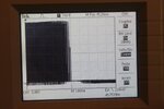
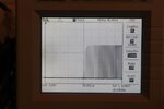
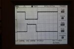
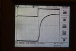
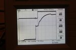
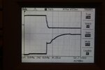
The thing is that as long as there's no load, the gates' waveforms are fine. But when I hook up the transformer, the signals that belong to the high side of both IR2110s star to behave in a strange way.
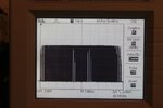
IGBT1.JPGIGBT2.JPGIGBT3.JPGIGBT4.JPG
As you can see, there is some kind of modulation issue.
The strange thing is that I replaced two IGBTs from one of the two IR2110s for two MOSFETS, and the problem is gone. While on the other IR2110 I still have the same problem on the high side gate.
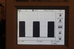
This is how the high side MOSFET behaves.
MOSFET1.JPGMOSFET2.JPGMOSFET3.JPGMOSFET4.jpg
Is this a layout problem (PCB stray inductance)? I know IGBTs have the "tail current" problem, but is this how they are supposed to work?
Any help or comment will be much appreciated.

Thanks very much in advance and happy new year!!

Martín
 

If I understand right, you are measuring high side gates (HO) against DC- (COM). That's the sum of bridge output and high side gate-source voltage and not actually a very specific waveform.

I don't understand however the voltage levels. We would expect slightly below 40 V output voltage plus e.g. 12V gate driver voltage. I see 35 respectively 22 V gate voltage level in the waveforms. Please explain the exact measurement conditions and probe connection.

Besides unexpected waveforms, which actual problems do you see in inverter operation? You didn't mention any.

You neither told about the involved modulation scheme. Is it suitable for reactive load?
 

FvM, thanks very much for your reply.
The pictures I posted were just figurative of the type of distortion I'm getting at the gates of the IGBTs placed on the high side.
I don't have at home a power supply capable of reaching 40Vdc, and since the H bridge starts working at 15Vdc, i thought it was ok to post them.
Regarding the PWM modulation scheme:
I used 200 values that correspond to half a cycle of a sine wave. This 200 values modulate the pulse width of the 20 khz signal.
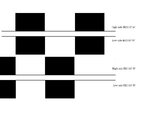
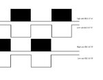
What comes out of the dsPIC is pretty much something like this:
mod.jpg

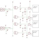
This two signals go into the optocouplers and go trough the following circuit:

schem.jpg

So, from the "pink signal", after the XOR gate, you end up with two signals that are complementary, and go to one IR2110 (A)
From the "blue signal" , after the XOR, you end up with another pair that are also complementary and go to the other IR2110 (B)
In the end, you have four signals (a pair that is complementary to each other and is 180 degrees apart from the other pair)
The comparators are there for adjusting dead time trough hardware to 1 uS.
I don't have any more pictures right now to post, but I'll get some later.
Thanks very much!!!!

Martín
 

You have clarified the modulation scheme and voltage level confusion, but didn't add anything about the observed problem. What I see from the post #1 waveforms is may be some instability with short on and off times. But it's impossible to distinguish between malfunction of the driver circuit and other possible reasons. My previous question still holds, do you see any irregularity in the output waveform or excessive output stage power dissipation?
 

FvM, first of all, I´d like to thank you for your time.
The AC sine wave at the output seems pretty much ok, although there's a small (very small) distortion approaching the the 0V crossing point.
I've been doing some measurements and tweaking the circuit a little with no results so far.
I've tried negative bias with no improvement, but while testing I came across what might seem the problem.
As I told you before, the modulation scheme might look something like this:
mod1.jpg

Now, I took some shots of the the signals at the HIN, LIN, HO and LO pins and saw something wired.

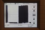
These are the two signals at the LIN and HIN pins. I've adjusted the deadtime to 2 uS. Top is HIN and bottom is LIN:
lowin_vs_highin.jpg

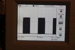
These are the signals at the HIN and HO pins without the transformer connected. HIN on top and HO on the bottom:
gatenoload_vs_inhigh.jpg

These are the signals at the same pins (HIN and HO) but with the transformer connected. As before, HIN on top and HO on the bottom.
Note that compared to the picture before, HO starts conducting before the HIN signal goes high):
gateload_vs_inhigh.jpg

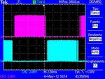
These are the signals at the HO and LO pins with the transformer connected.
Note that the HO pin goes high exactly at the same time the LO pin goes down, without the 2 uS of deadtime:
gate_high_vs_low.jpg

I guess this might be some sort of dv/dt problem. Technically the IRGP4063Ds come copacked with a diode. Is there anything I'm missing?
If I change the modulation scheme to something like instead o switching the low sides (at least that seems to be the problem) to 50 hz instead of 20 khz would make any difference?
That would look something like this:
mod2.jpg

Could this be a problem to the bootstrap technique?
Once again, thanks very much!!

Martín
 

Status
Not open for further replies.

Part and Inventory Search

Welcome to EDABoard.com

Sponsor

Back
Top