eztucker
Junior Member level 2
Hello,
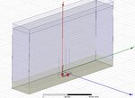
I have a very simple model, but I have attached a picture just to make it easier to understand. Basically, I have an airbox with a dielectric material at the bottom, which is sitting on a ground plane. There is a PML (set to be 1/10 of lambda) on the very top of the model. I am using plane wave excitation, normal to the structure (as you can see in the picture). NOT shown in the picture are different structures sitting on top of the dielectric at the dielectric/air interface. All I want to do is look at the wave front of the scattered radiation.
My question is where should I put the point "zero phase position"? Does it matter whether it is above the dielectric or maybe at the dielectric/ground plane interface? I have been debating with my lab mate about this for a while and we are interested to know if there is a difference. Thanks so much and look forward to your feedback
