Continue to Site

Welcome to EDAboard.com

Welcome to our site! EDAboard.com is an international Electronics Discussion Forum focused on EDA software, circuits, schematics, books, theory, papers, asic, pld, 8051, DSP, Network, RF, Analog Design, PCB, Service Manuals... and a whole lot more! To participate you need to register. Registration is free. Click here to register now.

How this circuit work?It puzzled me a whole night...T T

Status
Not open for further replies.

L_jack_xing

Junior Member level 2
Joined
Nov 16, 2013
Messages
24
Helped
0
Reputation
0
Reaction score
0
Trophy points
1
Activity points
186
I saw this curcuit in PI website.But I can't understand this
" As that difference exceeds about 100 mV, Q5 becomes biased off, which turns on Q4 and Q1 and allows current to flow from the 5 V output to 3.3 V output".
Please give me a hand if you can figure out .Thanks a lot:smile:.


Here is the article:

Active Shunt Regulator and Pre-load
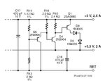
QQ截图20131209230343.jpg
Figure 1. Active shunt regulator for multiple output flyback converters

The circuit operates as follows. While the outputs are both within regulation, resistor divider R14 and R13 bias transistor Q5 on, which keeps Q4 and Q1 turned off. When in this mode of operation, the current through Q5 acts as a small pre-load for the 5 V output.
The nominal difference between the 5 V output and the 3.3 V output is 1.7 V. When the load demands additional current from the 3.3 V output without the same increase in load current being drawn from the 5 V output, its output voltage will increase with respect to that of the 3.3 V output. As that difference exceeds about 100 mV, Q5 becomes biased off, which turns on Q4 and Q1 and allows current to flow from the 5 V output to 3.3 V output. This current lowers the voltage of the 5 V output, which reduces the difference between the two outputs.
The amount of current that flows in Q1 is determined by the difference in the two voltages. Therefore, this circuit helps to keep both outputs in regulation, regardless of their loading; even in the worst case condition of the 3.3 V output being fully loaded while the 5 V output is unloaded. The arrangement of Q5 and Q4 provides temperature compensation, because the VBE temperature variations of each transistor cancel the other out. Diodes D8 and D9 are not required but reduce the dissipation in Q1, which removes the need for it to have a heatsink.
 

If I have this right, when the 3.3V line decreased due to load, Q4 begins to conduct due to it's emitter voltage drop, thus lowering Q5's emitter than it's base, therefore shutting it off
 

I think the 'shunt' it refers to is across the 5V and 3.3V lines and with around 1.3V lost in the diodes and 0.5V lost in the VCEsat of the 2SA0885, it isn't going to work very well. It's also worth noting that if the 3.3V supply is overloaded, both the diodes and the 2SA0885 are rated at 1A maximum and could therefore be damaged.

I think almost the same results could be achieved by using just two diodes and a resistor between the supplies.

Brian.
 

I understand your confusion. I don't think the description of how this circuit works is entirely accurate. This circuit works even if Q5 is not biased off. Let's take a look at what it would take to make Q5 get biased off. In particular, let's assume that the 5-volt output rail stays in regulation and it is only the 3.3-volt output that is subject to varying loads. The base of Q5 is fixed at 3.2 volts (assuming the 5 volt rail is in regulation). Q5 and R16 form a unity-gain emitter follower buffer. Whatever change there is in the voltage at the base of Q4, there is going to be at least 20 times as much change in the voltage at the collector of Q4 because of the beta of Q4. Therefore Q4 and Q1 will turn on or off with only a very small change in the voltage at the base of Q4. This change in voltage is not going to be enough to turn Q5 off. In fact, Q5 will merrily continue to conduct, providing a nice buffer and regulated 3.9 volts regardless of what changes there are in the loading of the the supplies. In fact the only thing that changes when the 3.3 volt output attempts to drop is the Q4 will turn on, not because its base is getting higher, but because its emitter is getting lower. Its base, remember, is the fixed 3.9 regulated voltage. So if the 3.3 volt output drops, Q1 turns on an feeds the 3.3 rail from the 5-v rail, which should help to stop the drop in voltage of the 3.3 volt rail.

Note that this circuit does nothing to stop a drop in both outputs together. If you imagine a proportional drop in both the 5-volt and the 3.3-volt outputs, the transistors will not turn on or off more or less. All that matters is the relationship between the emitter and the base of Q4. And that is dependent mostly on the ratio of the two output voltages, as determined by the R13/R14 voltage divider.
 
Last edited:
This circuit is a good idea to solve the cross-regulation problem on flyback converters, but as Tunelabguy mentions, does require further polishing.
 

Thanks first.But I am more confused about wether Q5 off or not after look through what Tunelabguy said downstairs.So I intend to do some experiments after.

- - - Updated - - -

Yeah.I want to replace that part with some elements.Making the unregulated output take more load.The rising voltage will decline,I see.

- - - Updated - - -

Thank you very much for explaining deeply ,so I get more information form the circuit.But there is a think that if the Q5 off or not still confuse me.When the Q4 conduct,the voltage at the collector of Q5 go down and below the base voltage.Then it biased off,isn't it?

And in fact,I want to alter this circuit for the feature:The regulated rail 5V fullload and the unregulated rail 15V unload.The 15V will soar high and "active shunt" work put the voltage down.When both 5V and 15V output unload or load in balanced.The "active shunt" do not work. Is it feasible in your opinion?

Thanks for your help again.

- - - Updated - - -

yeah,I will do some experiments after.I think it will solve a lot of project problem if it work well.:-D
 

Tunelabguy is correct, Q5's emitter wont drop, because its is fixed at 3.9V, it will always be on
 

Why Q4's on would not put the voltage at emitter of Q5 down?
 

Why Q4's on would not put the voltage at emitter of Q5 down?

Because as soon as Q4 turns on, Q1 also turns on. The moment Q1 turned on, it sources 3.3V to the 3.3V rail, which the emitter of Q4 rest upon. So now Q4 base has to be at 3.3V + 0.7Vbe - 2Vce = ~ 3.8V. Therefore Q5's emitter will always be at 3.8V
 

Oh,I saw the datasheet today and found BJT off just when the Ibe decline very low.So the Q5 would on all along.I think I have to review the theory of BJT again.Thank you.
 

Why Q4's on would not put the voltage at emitter of Q5 down?
When Q4 turns on, all that happens is that current flows from the collector to the emitter of Q4. Very little current flows in the base of Q4 to make this happen. The amount of current flowing in the base is so small that it has very little effect on the total current through R16, so the voltage at the end of R16 can stay the same and Q5 can stay on.
 

When Q4 turns on, all that happens is that current flows from the collector to the emitter of Q4. Very little current flows in the base of Q4 to make this happen. The amount of current flowing in the base is so small that it has very little effect on the total current through R16, so the voltage at the end of R16 can stay the same and Q5 can stay on.

Even if this base current flow is large, Q4's emitter voltage, which is set a 3.3V will prevent Q4 from lowering its base voltage
 

While output voltages are within limits current of Q5 is only 580uA and Q4 and Q1 are off. If 3.3V output is lowered for 100mV because increased current draw and 5V output remains unchanged base current of Q4 increases shutting down Q5 and turning on Q4 and Q1. Current from 5 V output is flowing to 3.3 V output. This current lowers the voltage of the 5 V output, which reduces the difference between the two outputs.

**broken link removed**
http://www.powerint.com/sites/default/files/PDFFiles/epr32.pdf
 

I have read these argticles before but could not understand what it said.Now I know more about how the circuit work.Thank you.
 

Status
Not open for further replies.

Similar threads

Part and Inventory Search

Welcome to EDABoard.com

Sponsor

Back
Top