Continue to Site

Welcome to EDAboard.com

Welcome to our site! EDAboard.com is an international Electronics Discussion Forum focused on EDA software, circuits, schematics, books, theory, papers, asic, pld, 8051, DSP, Network, RF, Analog Design, PCB, Service Manuals... and a whole lot more! To participate you need to register. Registration is free. Click here to register now.

com port on pcb proteus - package not found?

Status
Not open for further replies.

daddy1

Newbie level 3
Joined
Nov 11, 2013
Messages
4
Helped
0
Reputation
0
Reaction score
0
Trophy points
1
Activity points
22
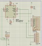
Hi, I tried to design a PCB and schema containing serial COM port, in design mode i can't find COM capsule, there is a solution?
In addition to what I wrote above i get some error messages in pcb design (design rule error DCR)
 

Attachments

  • plpcb-test.zip
    29.1 KB · Views: 94
  • plpcb-test.zip
    43.4 KB · Views: 82
Last edited:

If you mean the SMD pad clearance error then you can change the clearance in technology -> design rule manager , set pad to pad to 9th and you will be fine.
 

don't work a few errors only was removed...
 

The layout you have posted has several tracks crossing each other, unless you fix that how do you expect all the errors to go away?

Simple solution, delete all the tracks and use auto-router but don't expect much from this automated procedure

- - - Updated - - -

Snap2.gif

Here is what I mean by tracks crossing each other
 

The layout you have posted has several tracks crossing each other, unless you fix that how do you expect all the errors to go away?

Simple solution, delete all the tracks and use auto-router but don't expect much from this automated procedure

dont work with automated procedure error remain, i should use jumpers....? you have run the file attached?
 

select the track mode, then select all the tracks by click dragging over the entire pcb and press delete then autoroute
 

i will try tanks any solutions with com port pins over PCB?
 

you could use the D-type connector for the PCB and COMPIM for the simulation
the two components are connected in cascade mode.
DB9-01.jpgdb9-02.jpg
 

Status
Not open for further replies.

Part and Inventory Search

Welcome to EDABoard.com

Sponsor

Back
Top