Continue to Site

Welcome to EDAboard.com

Welcome to our site! EDAboard.com is an international Electronics Discussion Forum focused on EDA software, circuits, schematics, books, theory, papers, asic, pld, 8051, DSP, Network, RF, Analog Design, PCB, Service Manuals... and a whole lot more! To participate you need to register. Registration is free. Click here to register now.

[SOLVED] The PSRR of LDO circuit great than 1

Status
Not open for further replies.

Josephchiang

Member level 1
Joined
Oct 2, 2013
Messages
38
Helped
0
Reputation
0
Reaction score
0
Trophy points
6
Location
Hsinchu, Taiwan, Taiwan
Activity points
400
Dear all,

I design a Low dropout voltage(LDO) regulator recently.

But I doubt that my design will work when I see the PSRR simulation result.

The simulator which I adopted is Hspice.

I set the supply voltage vdd with dc bias voltage plus ac singal (V_PSRR vdd gnd dc vdd ac=1v)

After running the ac simulation,I probed the output terminal and found that the output ac value is great than one in the frequency of unit-gain bandwidth of Error amplifier.But the trend of curve seems right.

What's the potential reasons for that. Does the PSRR great than 1 is reasonable in LDO circuit?

The simulation result is shown as attachment.(There are three variation on the simulation,including output loading, Supply voltage, temperature hence total have 8 results in the same plot)
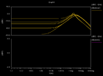
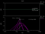
LDO_PSRR1.png

LDO_PSRR.png

The schematic of my design also shown in here. (The bias circuit in not shown in the schematic)

LDO_schematic.png

Any help is really appreciated,

Thanks
 

This is always one of the struggles with a PMOS LDO.
And try it with a PNP sometime. Any "groundward drag"
on the final gate is Miller amplified. And not attenuated
like your explicit comp network.

More shunt C from the final gate to VDD would maybe
help, like replacing the Miller comp with shunt comp. A
big area hit perhaps, but maybe a better behaving amp.
But this has always just been cut-and-try for me, no
sophisticated methods here.
 

By the way,for the special application the maximum supply current of LDO is only limited to 200uA.
So the heavy loading of 200uA and light loading of 20uA is applied here.
I doubt that the reason for PSRR higher than 1 is due to the low supply current of LDO.

- - - Updated - - -

This is always one of the struggles with a PMOS LDO.
And try it with a PNP sometime. Any "groundward drag"
on the final gate is Miller amplified. And not attenuated
like your explicit comp network.

More shunt C from the final gate to VDD would maybe
help, like replacing the Miller comp with shunt comp. A
big area hit perhaps, but maybe a better behaving amp.
But this has always just been cut-and-try for me, no
sophisticated methods here.

Thanks for your reply, dick_freebird.

I have a little confusion about your description.

Sorry , my native language is not English.

Could you express more detail for me.

What is the "groundward drag" ? Does the term "final gate" is refer to "gate of power mos"

"More shunt C from the final gate to VDD would maybe help, like replacing the Miller comp with shunt comp." Does it mean to use shunt capacitor from gate of POWER mos to VDD instead of the miller compensation network. Or both of them exist simultaneously?

Thanks
 

exemple power management project
I need a theoretical part of a voltage regulator(Low dropOut)-based technology CMOS ?
plz HELP ?
 

Hi Joseph,

PSRR need to be improved in your circuit .... LDO is a voltage regulator that means what ever be the power supply its output will not vary ... that is the essence of PSRR .... It generally comes with the specification of an LDO .... try to keep the peak below -10dB to -12dB... There are High PSRR LDO papers over net please go through them if possible .... such LDOs claim around max -40dB PSR.

In PMOS based LDOs we generally try to have a bad PSR for the error amplifier .... so that the PMOS gate has supply ripples .... The source is any ways connected to the supply .... if we manage to couple the supply variation at the gate as well then effective VSG remains same .... so no change in current supplied by the PMOS and hence no change in output .... that means good PSRR ...

But in your circuit the error amplifier is cascoded so it is having good PSRR ... that means the PMOS gate node is not receiving the supply changes ... therefore the over all PSRR is bad for your LDO... again Miller compensation reduces high frequency PSRR ... Try to use capacitor from the gate of the PMOS to supply this will help in coupling supply to the gate and also helps in compensation (but using only this for compensation will require a high cap value so you may have to think some thing more..... why not introduce a zero in the loop.... ;) ....)

Hope this helps ... :D

Thanks a million, SIDDHARTHA HAZRA

I think you must be a expert in this field

As your said, the output noise of error amplifier and power supply noise should be the same if PMOS based LDO was chosed

I don't quite understand about your description "But in your circuit the error amplifier is cascoded so it is having good PSRR ... that means the PMOS gate node is not receiving the supply changes ... "

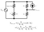
So I did the following simple analysis.

Both R1 , R2 represent the output resistance of cascode topology , assume R2 >> 2/gm

圖片 2.jpg

The result show that ac response of Verror_out/Vac=1

Could you explain more detail

I look forward to your response
 

As your said, the output noise of error amplifier and power supply noise should be the same if PMOS based LDO was chosed
I don't quite understand about your description "But in your circuit the error amplifier is cascoded so it is having good PSRR ... that means the PMOS gate node is not receiving the supply changes ... "
So I did the following simple analysis.

In order to understand my point lets take an example of a stand alone PMOS. We will discuss two cases:
CASE 1: The source of the PMOS is connected to a noisy supply and the gate is connected to a clean voltage. So VSG of the PMOS is varying continuously. Or in other words the current through it is varying continuously.
Now if we have a R load attached then the voltage at the output will also vary continuously as Vout(t) = I(t) * R or Vout(t) = [ K ( VSG(t) - Vthp )^2 ] * R . So PSRR will be poor.

CASE 2: The source of the PMOS is connected to a noisy supply and the gate is connected a voltage which is some how coupled with the supply i.e. It has similar variations as the supply. Then the VSG is fairly constant.
So is the current. The PSRR is good in this case.

Same is applied for the LDO. If the error amplifier has poor PSRR then its output will contain supply ripples. Now as this output is driving the gate node of the PMOS so the supply ripples are present at the gate node as well. This means VG is varying almost equally as VS is varying ... keeping VSG fairly constant .... and improving PSRR...

NMOS differential amplifier with cascode PMOS load has better supply PSRR than with single PMOS load ....

Hope this helps ... :)


Thanks for your detailed explanation

It's really helpful for me.
 

Status
Not open for further replies.

Similar threads

Part and Inventory Search

Welcome to EDABoard.com

Sponsor

Back
Top