Continue to Site

Welcome to EDAboard.com

Welcome to our site! EDAboard.com is an international Electronics Discussion Forum focused on EDA software, circuits, schematics, books, theory, papers, asic, pld, 8051, DSP, Network, RF, Analog Design, PCB, Service Manuals... and a whole lot more! To participate you need to register. Registration is free. Click here to register now.

[SOLVED] Circuit Design using logic Gates

Status
Not open for further replies.

slyfth

Junior Member level 2
Joined
Oct 13, 2013
Messages
24
Helped
0
Reputation
0
Reaction score
0
Trophy points
1
Activity points
232
Hi fellow professionals/students, this is my first post here on eda. I am stuck at a place where I have no idea on how to proceed.

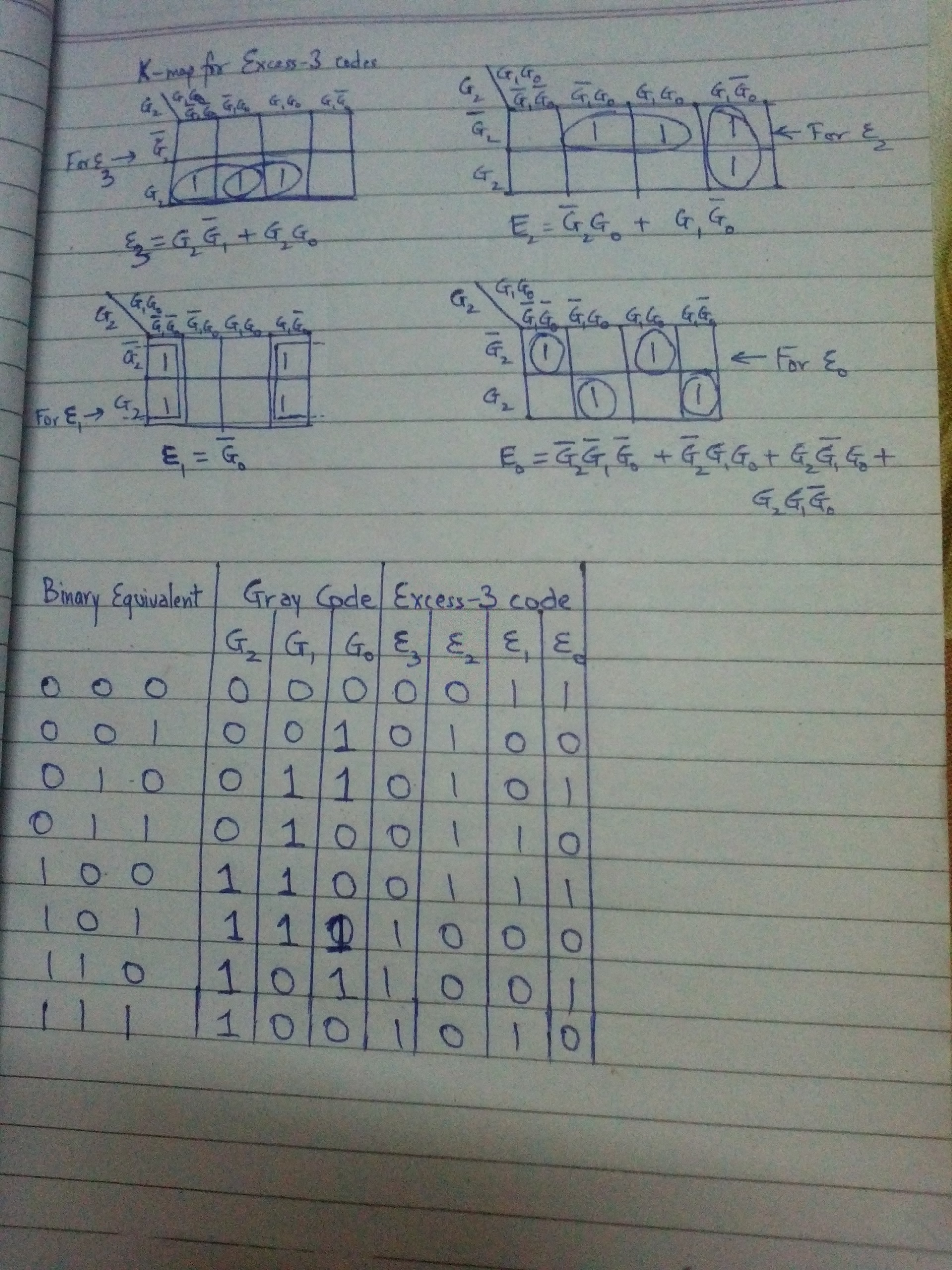
The problem is that I have to design a gray code to excess-3 converter using only NAND (IC 7000) gates. If someone can guide me on how to proceed, it'll be really helpful. Thanks in advance.

Regards
 

How far have you got yourself? have you drawn a circuit diagram?
 

I have gotten as far as understanding the logic behind Gray to BCD and then BCD to Excess-3 conversion. I have the truth table for Gray to Excess-3 code converter. I have the Boolean Algebra around it too but this doesn't solve the purpose. As it uses XOR gates and I was thinking if I need I will have to design each XOR gate as a NAND gate, it will be quite lengthy and a very complicated circuit. I know I have to play around with the Boolean Algebra and get to somewhere where it is all about NAND gates. A little guidance there will definitely be great.
Here is what I have got to play around with.
Gray to Excess-3.JPG
 

Shouldn't that be in your textbook as well somewhere? Input: truth table + logic element type available, Output: logic mapped onto said logic element.
 

@mrflibble
No, there's nothing like in the text-book(s) that I am referring to and we didn't have any such thing discussed in lectures either. Text book I am referring to are Thomas L. Floyd and John F. Wakerly. If there's a particular text book I can refer, please direct me to. Google's not helping with this.
All help is much appreciated.
 

Google terms du jour:
karnaugh map nand reduction
karnaugh map rolling nand
 

Don't focus on the NAND gates now. Use XOR gates and whatever you need to solve the problem. When you have the solution, implement all gates/blocks with NAND gates. You didn't say if you must use only 2-input NAND gates, or if the can have any number of inputs. It doesn't matter much for the problem solving, but you will have more drawing work in the final stage with only 2-input NAND gates.

Edit:
If you are supposed to solve the problem with Karnaugh maps you should not do what I suggested. With my solution you will get a block diagram that is possible to understand. You need very few block types for the solution. One of them is an XOR gate.

With the Karnaugh maps you will probably use fewer gates, but it will be a completely incomprehensible block of random logic.
 
Last edited:

The K-map suggestion was based on an assumption. My assumption was that this is a homework assignment. :p So I kept to the letter of the requirement, instead of providing more sane implementation options. ;)

Fits all the characteristics of homework:
- low post count
- curious requirements you only encounter for educational purposes

Actually now that I think about it, it's missing something. It doesn't include the typical "I need this ASAP! PLz be sending me the code mustafa_lzy@hotmail.com kthxbye!". And thanks for that. :)

Anyways, first implementing with XOR and then translating every XOR into a NAND will result in a crapload of NANDs. Then again, the requirements didn't specify you should use only the minimal amount possible. Soooo, that should work as well. :) So std_match's suggestion makes sense to try first. That will probably be easier.

Out of interest, does anyone know of any good Karnaugh map solver tools? I usually just do what everyone else does (leave it to the synth tools), but sometimes when I reaaaally want to get some performance I'll do it a la pen + paper. A tool to explore K-maps would every now and then save some time. So any good ones? Can be either windows or linux.
 

@std_match
This is a project from school. I am allowed to use IC-7000 2-input NAND gates, 5V Supply, a breadboard(of course).
@mrflibble
LOL! I don't do that "I need this ASAP! PLz be sending me the code mustafa_lzy@hotmail.com kthxbye!". Sounds more like a 10 year old girl. :p
I still have no idea on how to proceed from here, though I am a tiny bit smarter than before I started this forum, where I know that I write down equations for the conversion using any gate - XOR/AND/OR, but then where to from there?

Edit:
I was wondering if it will work if I first do the Gray code to Binary conversion and then Binary to Excess-3? Will that be a faesible way to proceed with things? Suggestions, please!
 

@std_match
LOL! I don't do that "I need this ASAP! PLz be sending me the code mustafa_lzy@hotmail.com kthxbye!". Sounds more like a 10 year old girl. :p

You'd be surprised at the amount of posts we get here from 10 year old girls wanting help with their electronic engineering homework.

I still have no idea on how to proceed from here, though I am a tiny bit smarter than before I started this forum, where I know that I write down equations for the conversion using any gate - XOR/AND/OR, but then where to from there?

Okay, I'll give you two hints. Look at it one output bit at a time.

Input G2,G1,G0 ==> Output E0. Start with a 3-input XOR gate...

Output E1 is possibly the simplest of them all. You'll need an inverter.. So E1 = ~ (something)

This is following std_match's suggestion of just trying to get the correct output using any standard gate that you need, and work your way from there.
 
  • Like
Reactions: slyfth

    slyfth

    Points: 2
    Helpful Answer Positive Rating
You'd be surprised at the amount of posts we get here from 10 year old girls wanting help with their electronic engineering homework.

I come across many such 10-year old girls on XDA and other forums too. Oh well, let's hope the World will grow up one day and there won't be any 10-year old girls left. :p

I have done something following your suggestions in the last post. However, it is not for a 3 I/P XOR gate.


I hope the picture is legible!

I have simplified the problem to simple equations using K-map. However, now I have no idea on how to convert these to 2 I/P NAND-only equations! Any ideas - on the process for doing so? or a book which can help me learn it simple like a, b, c? :)
 

You need the inverted version of some input signals. It is easy to use a 2-input NAND gate as an inverter.
Remember that a 2-input NAND gate can be viewed as a 2-input NOR with inverted signals. It is then very easy to design a circuit for y = ab + cd.
The problem is the E0 output. You can design wider NAND-gates by using multiple 2-input NAND gates, but it will be a mess.
The simplest solution for the E0 output is to use XOR gates and then convert them individually to 2-input NAND gates.
 

I'll give this a try over the weekend once I'm home.
 

I understand that for E3 and E2, it is will be an active use of NOT gates and OR gates, while for E1 it is simple NOT gate applied to G0. But for E0, I'm not able to simplify it further than = 'G2 AND (G0 XOR G1) OR [(G1 AND G0) OR ('G1 AND 'G0)] which is also equal to 'G2(G0 XOR G1) + 'G2(G2G1 + 'G2'G1). Can someone please help me simplify this equation further? I know that at some point in the simplification process, I need to use the formula (A + AB = B or, A + 'A'B = A + B), but how, I have no idea. Some help please?

Edit1: As for the NOT and OR gates, obviously, those will be the simple combination of NAND gates because that is what the main requirement is.

Edit2: OK, something happened and I just got smarter. I managed to simplify it one more step to get to E0 = G2 AND (G0 XOR G1) OR 'G2 AND (G0 XOR 'G1) = G2(G0 XOR G1) + 'G2(G0 XOR 'G1). (I think it might be incorrect because I believe the equation should be balanced in G0, G1 and G2, but it isn't. So maybe a calculation error on my end, please check).
I still need help to be able to implement this with the help of 2 I/P NAND gates.

Edit3: So, I have been able to get the design of the logic circuit diagram which only uses 2 I/P NAND gates, but I got a software to do it for me. I know in this e-age, it's fine to use these things to help you, but I have an ideology that until and unless I can solve the problem using plain 'ol paper and pen, I haven't learnt anything and hence haven't understood it. These softwares are there to make us smart, not dumb. So, I'll really appreciate if someone can teach me here as to how to reduce a boolean expression to the logic GATE of our requirement. (NAND in this case). It can't be impossible. Afterall, softwares must also be using some logic/reasoning to do it. I desire to learn that concept.:|
 
Last edited:

I don't know a general method for converting logic equations to a minimum number of 2-input NAND gates. As the logic size increases, the problem will quickly grow too complex for a human, especially if you have more than one output and want to minimize to total number of gates.

In this special case, I think I know the minimum solution for generating E0 from G0,G1,G2:
E0 = not (G0 xor G1 xor G2), which can be implemented with 9 2-input NAND gates.

Edit:
The total number of gates can be optimized. As an example, one gate can be removed from the E0 circuit by using E1 instead of G0.
 
  • Like
Reactions: slyfth

    slyfth

    Points: 2
    Helpful Answer Positive Rating
@std_match
Somewhat helpful. I'll do my own reading and try to find out an answer, will post it here, but that won't be until December I believe. I (the software) managed to design the conversion for all G0, G1 and G2 using 16 NAND gates in total. That's the minimum it uses. So that's 4 IC's on a micro breadboard. It'll be quite a mess for someone like me. :p
 

I (the software) managed to design the conversion for all G0, G1 and G2 using 16 NAND gates in total.
16 sounds like a good minimum when doing global optimization (sharing gates between the outputs). What software did you use for this?

I get 3 NAND gates to invert all of G0,G1,G2, this will also generate E1
3 additional NAND gates to generate E2
3 additional NAND gates for E3
8 additional NAND gates for E0 (the 9th I mentioned earlier is not needed since we now have the inverted signals available)

This is 17, but one NAND gate can be shared between E0 and one of (E2,E3).
 
  • Like
Reactions: zel

    zel

    Points: 2
    Helpful Answer Positive Rating
Apologises to everyone for being away from the board for so long. Had some work to attend to. Coming to the point:
The software I used for my task is Logic Friday. It is a freeware and can be easily downloded for Windows OS. I input the truth table in it and it gave me an output circuit of 16 NAND Gates because I mentioned that in the requirement check box that I require only NAND Gates used.

- - - Updated - - -

WOW!
I just realised that all this while I was quoting IC# 7400 as NAND gate when it is #7400 which is NAND. Stupid me!
 

Status
Not open for further replies.

Part and Inventory Search

Welcome to EDABoard.com

Sponsor

Back
Top