Continue to Site

Welcome to EDAboard.com

Welcome to our site! EDAboard.com is an international Electronics Discussion Forum focused on EDA software, circuits, schematics, books, theory, papers, asic, pld, 8051, DSP, Network, RF, Analog Design, PCB, Service Manuals... and a whole lot more! To participate you need to register. Registration is free. Click here to register now.

[SOLVED] Trouble with Delta Sigma ADC in FPGA

Status
Not open for further replies.

yhatagishi

Junior Member level 3
Joined
Apr 10, 2013
Messages
26
Helped
0
Reputation
0
Reaction score
0
Trophy points
1,281
Activity points
1,508
Hello all,


I want to realize delta-sigma ADC using FPGA, where digital processing (the cic filter) is implemented in FPGA and only R and C are the analog parts.
LVDS is used as comparator.
The block diagram is below.
block.png

The problem is that the ADC ouput is not what I expect.

- when voltage of inputs are below 0.5 V : output is 0 V
- when voltage of inputs are near 2.5 V : output seems to be saturated around 2 V

When they are in 0.5 - 2.0 V and above 2.7 V, the output seems fine.
I drew the simple diagram of the input and output (Sorry for my bad drawing).
drawing.png

I am pretty sure that cic filter is working fine.
I think LVDS is the one causing those problems for the voltage that causes problems is outside the common mode voltage.
But I do not know how to deal with it...

So I want to know how I can solve those problems.
Or if anyone knows what the real problem is, please tell me.


Best regards,

Yukihiro Hatagishi
 
Last edited:
Hi,

You crossscheck each stage's output .. this will help you to find the problem..

Thanks
 

Waht you obserev is the limited common mode range of the LVDS receiver. It's not designed as a comparator with rail-to-rail input range.
 
Dear kenambo,

thank you for your help.

I actually did crosscheck each stage and found out that FF is working odd.
So as I wrote and FvM mentioned below, I am thinking that LVDS is not working good.

I want to know how to make the LVDS work correctly...


Dear FvM,


Thank you again!!

OK, so your reply convinced me that common mode voltage range was the main factor.
However some of the websites introduce the delta sigma adc implemented in FPGA as useful...
That means there are some ways to overcome the problem, right??
I want to know it. Any ideas??

I've been pretty annoyed by this problem for like 1 month...


Best regards,

Yukihiro Hatagishi
 

Different FPGA families might have different common mode ranges.

You could try an "inverting" comparator configuration with one input biased to mid supply and input voltage and feedback summed by two resistors. Or use a voltage divider and reduced input voltage range.
 
Dear FvM,

thank you for your reply.

Different FPGA families might have different common mode ranges.
Oh, different LVDS may be the one... or maybe using LVPECL is also a solution.
How about the delta sigma ADC IP sold below here??
**broken link removed**
Is the IP is limited only in some FPGAs having wider common mode voltage?? What do you think??

You could try an "inverting" comparator configuration with one input biased to mid supply and input voltage and feedback summed by two resistors. Or use a voltage divider and reduced input voltage range.
You mention "real" delta sigma ADC.
I thought that one too but that changes the impedance of analog input...
Doesn't it (changing impedance) cause any trouble??


Best regards,

Yukihiro Hatagishi
 

You mention "real" delta sigma ADC.
I didn't yet. It would use an integrator front end with respective linearity.

I'm talking about possible modifications to the simplified SD frontend utilizing LVDS receivers. I have no idea if it gives noticeable improvements, just a suggestion to try out.
 

Dear FvM,

Thank you for your reply.
Sorry for my late reply.
I didn't yet. It would use an integrator front end with respective linearity.

I'm talking about possible modifications to the simplified SD frontend utilizing LVDS receivers. I have no idea if it gives noticeable improvements, just a suggestion to try out.

I will try it and report the result here.


Best regards,

Yukihiro Hatagishi
 

Hello all,


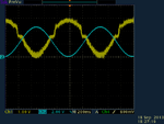
I tried the circuit FvM told me and I could get over the common mode range problem.
However, I still have a problem left. The waveform is shown below.
20130918_wave.PNG
Blue is the input sine wave of 1 Hz and the yellow is the output.

What causes the odd wave form??
and how can I process this digitally??


Best regards,

Yukihiro Hatagishi
 
Last edited:

Looks like you are trading one kind of nonlinearity against the other. Don't know how it happens, but it doesn't seem to be a promising way.
 

Dear FvM,


I found the strangeness of output waveform was due to the coupling.

After placing my analog circuits in appropriate position, DS ADC worked well (although there is an offset problem).


Thanks,

Yukihiro Hatagishi
 

Status
Not open for further replies.

Part and Inventory Search

Welcome to EDABoard.com

Sponsor

Back
Top